Lab4
Lambda : Reading Phototransistors on ADC Inputs: Logic for Rotation to Light
Source
Background: Here
you will use the two DAC channels on the 6024E card to send analog signals to
the MSP430 microcomputer. The analog signals will simulate the output of two phototransistors.
It will be imagined that PNZ150 phototransistors are responding to a distant light
source, as they did in Lab 2. Based on the sum and difference of the two analog
signals, the code will orient the (simulated) rover to point toward the light.
In essence, the phototransistor signals will act as FEEDBACK for the rover navigation
to knock over block under the lamp.
(You
are required here only to upgrade Lab4pre to handle analog IN and demo on the
LabVIEW exercise VI that your code logic works to respond properly to phototransistor
signals difference and sum.)
Requirements:
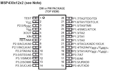
You must use an MSP430F1232 chip on the demo board; it will support the
successive approximation A-D conversion the code will be expecting.
(1)
"Upgrade" your Lab4pre to add two analog-out sliders: See suggestion:
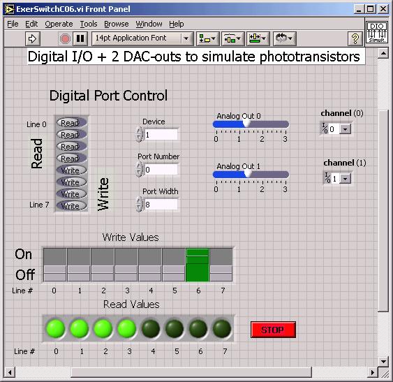
the sliders will have a range of 0-3volts, since the MSP430 will recognize
analog signals of no greater than 3v magnitude.
The
LEDs L0 to L3 represent what they did in Lab4pre:
L0
ON left wheel going forward; L0 OFF left wheel in reverse
L1 ON right wheel
going forward
L2 ON left motor turned ON; L2 OFF left motor inhibited
L3
ON right motor turned ON
The
switches D4-D6 act the same as they did in Lab4pre:
D4
ON implies rover is in contact with left wall
D5 ON implies rover is in contact
with right wall
D6 ON means the timed loop is activated inside the infinite
loop of the code.
(Flick D6 so the rover goes through only one cycle of 40
sec or so)
(2) Copy and rename the distribution
source code Lab4C06.c. Find modifed code in IAR 4.0 "workbench". The
following code to accommodate two channels of A-D conversion in the MSP430F1232
is added in
a version of Lab4pre default code are in source
code
Lab4C06.c, in
the EN123 IP
First, near the top of main()
declare
int photoL, photoR, thet_diff_LO, thet_diff_HI, thet_summ_LO,
thet_summ_HI;
signed int diff, summ;
These lines declare variables for the A-D conversion.
Second, just after the line
that has as a comment //stop Watchdog Timer enter
ADC10CTL0 = SREF_1+ ADC10SHT_2 + REFON + REF2_5V + ADC10ON
+ ADC10IE;
// ADC10ON, interrupt enabled, 2.5v reference
ADC10AE |= 0x03;
these lines help setup
the ADC registers.
Next you need to add, just
after entering the timed loop code,
ADC10CTL0 &=
~ENC; // have to disable ADC10 to change channel
ADC10CTL1= INCH_1; // ADC10MEM reads from A1, right side
ADC10CTL0 |= ENC + ADC10SC; // Sampling and conversion start
_BIS_SR(CPUOFF + GIE); // LPM0, ADC10_ISR will force exit
photoR = ADC10MEM; //record digital A1 into storage photoR
ADC10CTL0
&= ~ENC; // have to disable ADC10 to change channel
ADC10CTL1=INCH_0; ///ADC10MEM reads from A0, left side
ADC10CTL0 |= ENC + ADC10SC; // Sampling and conversion start
_BIS_SR(CPUOFF + GIE); // LPM0, ADC10_ISR will force exit
photoL = ADC10MEM; //record digital A0 into storage photoL
diff = photoL - photoR; // difference of photoxsistors
summ = photoL + photoR; // sum of photoxsistors
this code acquires the
two analog inputs and assigns their digital values to photoL and photoR.
Finally at the end of the
code, after the last curly bracket of main, add
#pragma
vector=ADC10_VECTOR
__interrupt void ADC10_ISR (void)
{
_BIC_SR_IRQ(CPUOFF); // Clear CPUOFF bit from 0(SR)
}
which is "magical
code" taken from a TI sample of how to carry out succ. approx A-D conversion.
It is basically an interrupt that starts the actual conversion.
Make sure you hit "Rebuild
All" frequently as you add this code...The A-D conversion won't run without
the last magical lines, so don't worry if a test on your board stalls without
the last lines above...
Note: The two A-D conversion
inputs are port 2.0 and 2.1 = pins 8 and 9 on the MSP430F1232 chip:
(3) As you remember from Lab4pre, a test of your VI will mean connections
on a NI green board of
DI/O 0 to DI/O 4
DI/O 1 to DI/O 5
DI/O 2 to DI/O 6
DI/O 3 to DI/O 7
To
test your "exercise" VI, declare (with switches) that bits 0-3 are
READ and 4-7 are WRITE.
and
After
testing use the 1232
demo board wired up the a green connector card now
sending LabVIEW DAC-out screw terminals 21 and 22 to MSP430 analog-in channels
P2.1 (pin 9) and P2.0 (pin 8. Check that the sliders are work to change a voltage
from 0 to 3v.
Reasonable threshold values,
in hex:
thet_diff_LO
= -0x04F; // or use 2's complement form for negative...
thet_diff_HI = 0x04F;
thet_summ_LO = 0x03F;
thet_summ_HI = 0x5FF;
2008:
actually, we will want thet_summ_LO to be represented by the hex code for 1
volt
and thet_summ_HI to be represented by the hex code for 4=2+2 volts...
(4) Next, modify code inside
your pp < pp_max timing loop such that (in psuedocode):
(i) If summ < thet_summ_LO
then
the simulator behaves just as it did for Lab4pre:
goes forward by default or turn when it hits a wall...
(this is the state of being too far away from the light source to care...)
(ii) If summ > thet_summ_LO
&& summ <thet_summ_HI
then
(iii) if diff < thet_diff_LO
(a negative number) then
(iv) turn CW until diff
> thet_diff_LO
&& diff
< thet_diff_HI
ELSE
(v)
If diff >thet_diff_HI
then
(vi) turn CCW until diff
> thet_diff_LO
&& diff
< thet_diff_HI
ELSE
(vii)
then go forward toward the light
(viii) if summ > thet_summ_HI
have
simulator
behave just as it did for Lab4pre
going forward unless it hits a wall...
(state of being too close to the light to make proper judgement...)
As
you make make the improvements above, frequently "Rebuild All". When
finished download the code into the MSP430F1232 using the DEBUG command. Either
single step through to debug or start and stop the debugging to test your code
in the VI exercise simulator.
You
may want to make sure you see the following connections of LabVIEW connector card
to MSP430 demo board:
D0 screw 52
to MSP430 pin 21 (P1.0) port 1/bit 0 is the LEFT motor direc
control
D1 screw 17 to MSP430 pin 22 (P1.1) OUT:
direc control for Right stepping motor
D2 screw 49 to MSP430 pin 17
(P3.6) output to inhibit motor,
Left
D3 screw 47 to MSP430 pin 18 (P3.7) " Right
D4 screw 19 to MSP430 pin 24 (P1.3) IN signal from lever
switch on rover, Left
D5 screw 51 to MSP430 pin 23 (P1.2) "
Right lever switch
D6 screw 16 to
MSP430 pin 11 (P3.0) IN signal from V-switch to start movement
sequence
D7 screw 48 to MSP430 pin 12 (P3.1)
(future wireless input) back up command
DAC-OUT-0
screw 22 to MSP430 pin 8 (P2.0) Left
phototransistor/slider
DAC-OUT-1
screw 21 to MSP430 pin
9 (P2.1) Right
phototransistor/slider
Green
GND wire of MSP430 board to pin 53 (GND) of the LabVIEW connector card.
(P1.4-7 on
the demo board are not available
to the user)
Possible FTQ: Explain how you read new analog values for the continued
testing in the logic for the light sum and difference testing. .
Free Advice: Consider describing your coding
problem as a series of STATE changes.
Consult the yellow IAR User Guide
for information about the features of the debugger, including single-stepping
through code.