Lab
ADA: Analog to Digital to Analog Conversion, 8-bit
Background: Any
analog signal sent into a computer must pass through an A-D converter. Lab ADA
explores the amplitude resolution and error aspects of A-D conversion, using
3 chips from Analog Devices of Norwood MA, and a 2-digit hex dot matrix display.
A digital-to-analog chip converts the digital of the ADC back to analog for
comparison.
Suggested Requirements:
Go to the Analog
Devices website http://www.analog.com
Access and print out the datasheets for the
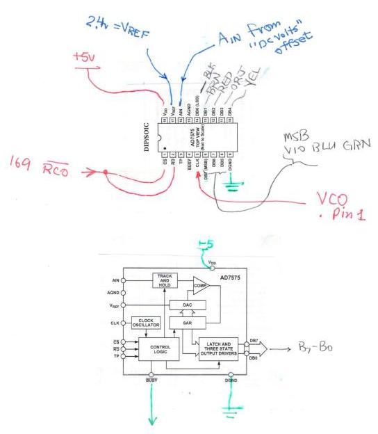
7575 8-bit A-D converter
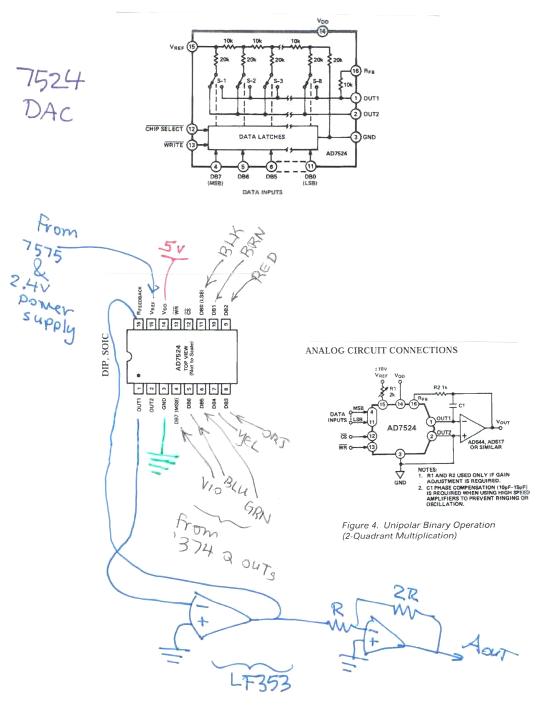
7524 R-2R ladder + switches to combine with LF353 op amps to form a multiplying
D to A converter.
AD654 Voltage-controlled oscillator
You will also
want data sheets for
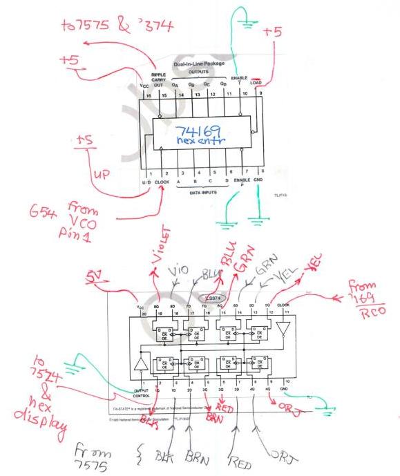
74LS169 4-bit counter (needed for its RCO/ output)
http://www.national.com/ds/54/54LS169.pdf#page=1
74LS374 8 bit latch (to capture the answer after 8 clock pulses to the 7575)
http://www.national.com/ds/DM/DM54LS373.pdf#page=1
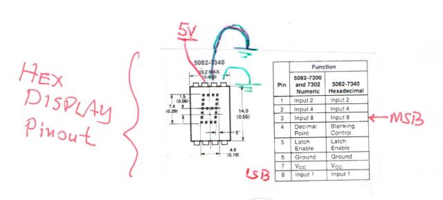
HP 7340 hex dot-matrix display (2 needed, for 8 bits of data)
http://www.viewcom.force9.co.uk/displays/Display-pdf/HP5082-73xx.pdf
note the pinout is a bottom view of the chip...
and you already are familiar with the LF353 op amp, needed in conjunction with AD7524.
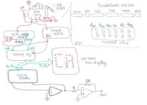
You will be given a blue box power supply with an "A 2 D 2 A" circuit using all the chips above. You will want to verify that the board is converting an analog input, displaying the conversion, then sending that digital representation to a DAC for output through a LF353.
See diagrams referenced below.
The
blue box will have a terminal block for
*Analog-in (pin 14, 7575)
*Analog-out (from inverting op amp of LF353)
*V-ref (pin 15, 7575,
*654 CLK pin 1
*RCO/--start-of-conversion pulse from pin 15 of 74LS169
*BUSY/ signal of 7575, pin 4.
Make sure ground of the blue
box supply is connected to ground of the 3631 Agilent supply.
Note that "Analog ground" pin on the 7575 chip is set to 0 volts (ground).
See from the 7575 data sheet that it takes 20 clock pulses to finish a conversion...odd, you'd expect 8 clock pulses if this were an 8 bit A-D succ approx at advertised...
(1) Verify that there are clock pulses on 654 pin 1, 74LS169 RCO/ and 7575 BUSY/ (use logic probe). Figure out the clock rate of BUSY/ using your o-scope. On the scope have traces for BUSY/ and CLK on the screen simultaneously. How many clock pulses per "BUSY"? What does the 7575 documentation say about how many clock pulses are needed for one conversion?
(2) Establish a V-ref of say 2.4 volts from the 6v tap on the Agilent 3631 power supply. Using the DC-volts capability of your 33120 function generator as Ain, verify, or arrange, that the A-D conversion on the HP7340 hex displays goes from 00 to FF as the DC volts is increased from 0 to about 5 volts. Can you still reach FF if V-ref is increased to 4.0 volts? Does the Aout from the second op amp track Ain?
(3) Send to Ain from the 33120 a triangle waveform of 2Hz, with an offset to keep its lowest level above 0 volts. Show the Ain on one channel and Aout from the 7524 on the other o-scope channel. Note a staircase waveform tracking the triangle wave. With the triangle waveform amplitude at about 200mV p-p, what is the resolution in mV of the A-D-A conversion (the step size of the analog staircase)? Is 256 times this resolution equal to 2*V-ref?
(4) What is the minimum (maximum) error (in terms of the LSB step size) on the analog-out tracking the triangle wave? Allow yourself to use to vertical position knob on the o-scope to line up Aout with Ain as best you can...
(5) "Strobing the triangle wave": You know the sample rate...it is the BUSY/ rate. Set the triangle waveform to the sample rate and adjust it by 0.1 Hz until the A-out is a flat line of "zero Hertz".
(6) Take the triangle wave back down to say 4 Hz. Use the FFT capability of the o-scope to look at the frequency response. Can you see 4Hz on the spectrum? What other frequencies are prominent? Can you see the sample rate?
(7) Multiplying DAC: Make sure the Ain is a triangle wave of 0-2.4v peak. Find the wire on pin 17 that chains from Vref of the 7575 to Vref of the 7524. Move the wire on the 7575 from Vref to Ain, pin 16. Now the DAC Vref will "multiply" the DAC inputs. You should see a parabolic Aout staircase that represents Ain(digital)*Ain(analog). Use a slow triangle wave going from 0 to 2.4v and back. Draw out what Aout looks like. Why are the "stair steps" not horizontal? Move the Vref wire back to pin 17 on the 7575 when you finish!
(8) Exponential decay with LabVIEW. Design a VI with 2 frames. In the first frame have 6024E analog out channel "0" be 4 volts for half a second, sent to Ain. the second frame will have a FOR loop running for 20 cycles, with a 500 msec WAIT time in each cycle. The loop will send an analog voltage out channel 0 to Ain of the blue box circuit board. On a 6024E analog-in channel the blue box Aout will be read, and sent to the second frame, where it will be multiplied by 0.92 and sent out the Aout. Show on a 20 second scope sweep the exponential decay of A-out. What happens to Aout if you set the multiplication factor to 1.0?
In (8) we employ the A-D converter of the 6024E Nat'l Inst. DAQ card, and the DAC of the 6024E card, so with 7575 and 7524 four converters are "in the loop" of the demo.
(9) (a) Bipolar operation: Study figures 15-18 on the AD7575 data sheet. In fig. 17, what is the gain of the "TLC271" op amp? Calculate: What happens at V+ of the op amp when input voltage is -5v? Work through the voltage dividers there...
(b) Study Fig 18 in the 7575 data sheet. In 2's complement code for representing signed binary numbers, a MSB of 1 represents a negative number and 1111 1111 is the code for -1. The largest positive number would be 0111 1111 = 7F. How could the 7575 code for bipolar be converted to 2's complement? In other words, looking at the 4-bit example below, what logic operation will transform 7575 code into 2's comp? Looking up 2's complement code on the internet, what computational advantage does it have over the 7575 code?
| Analog | 7575 code | 2's comp |
| 7 | 1 1 1 1 | 0 1 1 1 |
| 6 | 1 1 1 0 | 0 1 1 0 |
| 5 | 1 1 0 1 | 0 1 0 1 |
| 4 | 1 1 0 0 | 0 1 0 0 |
| 3 | 1 0 1 1 | 0 0 1 1 |
| 2 | 1 0 1 0 | 0 0 1 0 |
| 1 | 1 0 0 1 | 0 0 0 1 |
| 0 | 1 0 0 0 | 0 0 0 0 |
| -1 | 0 1 1 1 | 1 1 1 1 |
| -2 | 0 1 1 0 | 1 1 1 0 |
| -3 | 0 1 0 1 | 1 1 0 1 |
| -4 | 0 1 0 0 | 1 1 0 0 |
| -5 | 0 0 1 1 | 1 0 1 1 |
| -6 | 0 0 1 0 | 1 0 1 0 |
| -7 | 0 0 0 1 | 1 0 0 1 |
| -8 | 0 0 0 0 | 1 0 0 0 |
For all the questions above, enter answers for your team in a (word or excel) document that you preserve in your IP folder. Be prepared (as a team) to show three of the answers, such as (3),(5) and (8).
Notes: Here are circuit
diagrams that will be of interest to you in troubleshooting the FTQ:
Overall circuit diagram
AD654 VCO
7575 8-bit ADC
74169 hex counter with RCO/ and 74LS373
octal latch
HP7340 dot matrix hex display chip
7524 R2R ladder 8-bit multiplying DAC
FTQ: You will be asked to set up again the triangle wave
staircase situation (3, 7) above then turn your backs. We will move/remove a
few of the wires in the data path so there is a mistake in displaying the staircase.
You must figure out what wires were "rerouted" and restore the circuit
to proper action. Time limit 24 hours.