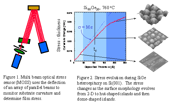
Multi-beam Optical Stress Sensor (MOSS) - MOSS is an optical technique for measuring stress in thin films by measuring the curvature of the wafer. By simultaneously measuring the deflection of an array of parallel beams (instead of moving the beam or the sample), the curvature can be measured with no moving parts. This approach significantly reduces the effect of sample vibration so that the system can be used in many processing environments with minimal modification (sputter deposition, molecular beam epitaxy, chemical vapor deposition). The system is capable of measuring radii of curvature as large as 20 kM which corresponds to a sensitivity in stress*thickness of 1 GPa-angstrom, i.e, we can measure the stress from less than 0.1 monolayer of Ge deposited on a Si(001) substrate.
We have used this technique to measure stress relaxation due to the formation of quantum dots, dislocation-mediated strain relaxation during semiconductor heteroepitaxy, residual stress evolution in metal polycrystalline films, high temperature CVD growth of GaN layers, sputter deposition and pulsed laser deposition of hard coatings. The data in figure 2 show the evolution of the stress as the surface morphology changes from a flat surface to a surface covered with islands.