We use our MOSS (multi-beam optical stress sensor) technique to measure the evolution of film stress in real-time during growth and processing. Development of analytical models for stress generation and relaxation are closely coupled with the experimental program. Current areas of interest are:
- Residual stress during film growth
- Stress from thin film reactions (Sn whisker formation)
- Stress during electrodeposition of thin films
Residual stress during film growth -
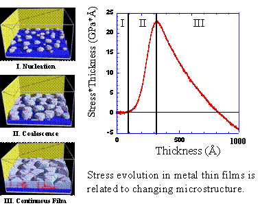
This effort is focused on understanding the mechanisms that generate stress in thin films during growth, corresponding to the different stages of microstructural evolution as shown in the figure. Measurements of film stress evolution are interpreted in terms of models including effects of growth kinetics. For example, we have proposed a model for the steady state compressive stress in metal films that is due to the non-equilibrium conditions on the surface during growth.
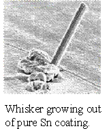
Stress from thin film reactions (Sn whisker formation) -
Sn coatings are used on Cu substrates to enhance solderability and prevent oxidation. When pure Sn coatings are used (i.e., without Pb) the layers develop whiskers. We are studying the process of whisker development to understand the driving forces and kinetic mechanisms controlling it and to develop alternative, whisker-free coatings.
Stress during electro-deposition of thin films –
The wafer curvature apparatus has been implemented on an electrochemical deposition system to study the evolution of stress in situ while films are deposited and etched.