

Distributed May 7, 2003 |
News Service Contact: Scott Turner
|
|||
|
Watching the flow of electricity New sensor bares faults in smallest possible, most advanced circuits Scientists at Brown University have created a magnetic-sensing microscope that allows them to watch electricity flow through the world’s tiniest components. They are using the device to find defects in integrated circuits and micromachinery. The design opens the door to wider application of magnetic-sensing technology for imaging electrical current flow. The microscope is described in the May 12, 2003, issue of Applied Physics Letters. PROVIDENCE, R.I. — A new scanning microscope developed at Brown University can uncover defects in the smallest and most complex integrated circuits at a resolution 1,000 times greater than current technology. The scanner removes a barrier to further shrinking of integrated circuits: As circuits get smaller, non-visual defects become harder to find. 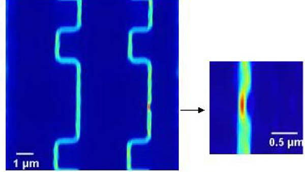
Micro mouse bite “This microscope will allow manufacturers to find defects in each embedded wire in ever-tinier circuits,” said Brown University professor Gang Xiao. He developed the instrument’s hardware and software with Ben Schrag, who will receive his Ph.D. at Brown this month. The microscope’s magnetic-scanning technology suggests a new small, non-invasive form of remote detection, said the researchers, who envision a “pass-over and detect” magnetic-sensor-tipped pen, for use in finding internal cracks within aircraft, sensing biological agents in the environment or body, or recognizing counterfeit bills or other objects. Although magnetic sensing is used extensively, it is not applied widely for imaging electrical current flow, said Schrag. The only method that uses magnetic imaging to see current flow is restricted to extremely low temperatures, employing cryogenic aids such as liquid nitrogen. However, the Brown device works at room temperature. This design opens the way to greater use of magnetic sensing technology, he said. “The factor of 1,000 improvement in spatial resolution is how much better we can do than this cryogenic technology,” Schrag said. “We are just scratching the surface of potential applications.” Xiao and Schrag are using the technology to pinpoint how electrical current can form pinholes in state-of-the-art devices called magnetic tunnel junctions. These tiny sandwiches of ferromagnetic layers and insulating material are candidate memory storage cells to replace standard cells used in computer memory chips. The researchers have “imaged” current flow in electrical components as small as 50 nanometers, the smallest commercially available components, half the size of conventional chips. Until now, little or no technology existed for actually “watching” electrical current flow, said Schrag. Whenever current runs through wires, such as those embedded within the semiconducting material of an integrated circuit, it creates a magnetic field. By measuring spatial changes in that magnetic field, the microscope visualizes electrical current, even within wires buried under layers of advanced materials, he said. “The device allows us to see the evolution of hot spots on each wire in a circuit and how each defect moves down the wire in the form of electrons moving atoms,” said Xiao. “To see a collection of atoms moving as a function of time is a capability that did not exist until now. We are witnessing the flow of electricity. It appears similar to an image of human blood flowing.” The microscope is described in a paper in the May 12, 2003, issue of Applied Physics Letters. It features some of the same magnetic-scanning technology found in computer hard drives. A scanner does not touch what it reads. Instead, a magnetic sensor the size of a small pea moves quickly back and forth over a circuit through which current flows. The sensor collects information, which is then converted by algorithms into a color picture of electron flow. Color changes in the image reflect the intensity of electron flow as well as the presence of defects. About the size of a refrigerator, the microscope is being reduced to the size of a desktop computer. “The new design will allow a technician to sit in front of a monitoring screen, as integrated circuits pass through a small open door, under a scanner and out the door,” Xiao said. Currently, the microscope takes a few minutes to scan a circuit. The researchers are working to reduce that time to as little as 30 seconds. Xiao and Schrag have filed patents on several aspects of the technology, which has been transferred to Micro Magnetics, a Fall River, Mass., company that makes scanning devices for manufacturers of integrated circuits (computer chips). Images produced by the microscope may be viewed at http://www.micromagnetics.com/. The National Science Foundation funded this work. ###### | ||||
 |
 |
 |
 | |