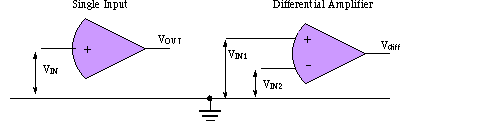
where VIN1 and VIN2 are two inputs, subtracted.
In a real circuit, the gain will be frequency dependent, but let us start with consideration of the gain in an ideal amplifier.
Overview
You are first shown good reasons for amplifiers to be included in instrumentation systems. Next various off-the-shelf amplifiers are explained, and you learn how to adjust the gains of these amplifiers for your particular purposes.
Amplifier specifications: Gain, Gain-Bandwidth Product, Common-Mode Rejection Ratio, Settling Time, Input Impedance, etc are explained and compared for different categories of amplifier. Gain as a function of frequency is dealt with in particular.
The operational amplifier is considered in detail, and you learn to be comfortable with the negative gain summation amplifier circuit, and learn how it can be used to create a rough-and-ready D-A converter. You also learn that the Unity Gain Voltage Follower op amp circuit is a standard isolator between sensors and further amplification.
Why amplify
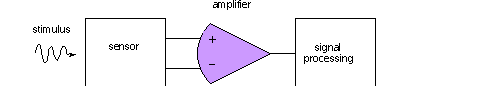
As you learned in Chapter 1, an electronic instrumentation system employs sensors that report their outputs as voltage. In some cases the output of a sensor may be only millivolts in amplitude. In order to see the sensor signal on an oscilloscope or convert it to digital form, the signal must be amplified. Sometimes the unstimulated sensor output is brought to zero by an offset circuit, such as a Wheatstone bridge for strain gauges. Again, in this case, an amplifier is called for.
You as the designer of the system likely want some control over the amplitude of the output, and therefore are motivated to learn about circuits that provide voltage gain; such circuits are called amplifiers.
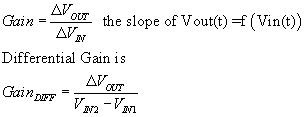
Gain
Gain is the ratio of output voltage to input voltage
of an amplifier,
where VIN1 and VIN2 are two inputs, subtracted.
In a real circuit, the gain will be frequency dependent, but let us start with consideration
of the gain in an ideal amplifier.
The ideal amplifier
An ideal amplifier will pass the input signal through to the output undistorted but enlarged (gain set by user), with no delay. It will not be affected by the output impedance of the source (sensor). In addition the ideal amplifier will be able to drive any load: supply any current.
No real amplifier is ideal, but an op amp can come close, at least with regard to gain at low frequency. The typical IC op amp has an open loop gain of 10^6 and a low frequency input impedance of about 10^12 ohms. We'll see shortly how such high open loop gain is harnessed to create user-desired gains.
Nonlinear gain: Consider log amplifiers and "anti-log" amplifiers: for enhancing or minimizing waveform "spikes". Filtering by amplitude. In Simulink: the Deadzone operator.
Off-the-shelf amplifiers
In this chapter you will learn how to apply off-the-shelf amplifier ICs (integrated circuits) to problems in instrumentation. First will come operational amplifiers (op amps)--the most ubiquitous linear IC in the world--then instrumentation amplifiers that are optimized for true differential gain, then isolation amplifiers, designed to prevent noise and unwanted current from moving between sensors and downstream signal processing components.
In this chapter we will consider three particular IC amplifiers:
Op amp National Semiconductor LF353
Instrumentation amp Analog Devices 524AD
Isolation amplifier Analog Devices 202AD
The first two chips are also used in the lab component of Instrumentation: From Sensors to
Software.
You will learn to apply these amplifier ICs to your instrumentation problems by modifying (or selecting) the gains of the IC amplifiers.
Basic amplifier specifications
For an instrumentation system builder it's not enough to know that you need an
amplifier: You need to understand the interface at the sensor- amplifier input connection,
and the signal processing destination of the amplifier output:
Subsequent chapters will deal with specific sensors and with signal processing (filtering);
for now assume the amplifier you are to work with has already been designed and
packaged, and your job is to match the specifications (specs) of such an amplifier
to the particular design you're working on.
As you can tell by inspecting the data sheet for an IC amplifier, there are many specification parameters; one way to classify the parameters: static vs dynamic characteristics. To begin with, we will consider gain, in both static and dynamic forms.
Because there is nonzero delay from input to output in an
amplifier, the gain can be expressed as a ratio of peak or average output to
input, when the input is a sinusoid.
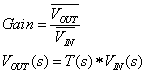
where the bar represents average of a signal. Gain is embedded in the frequency-dependent
transfer function T(s).
In fact gain is frequency dependent, and the amplifiers considered here can be characterized by a gain-bandwidth product. The data sheet can show a graph of gain vs bandwidth that illustrates the gain-bandwidth product. The GBP for the LF353 is 4 MHz, for example. The gain falls off as if the op amp has a first order low pass filter in it. That is, the gain decreases at 20 dB per decade. Recall the definition of decibel! 20 log10(gain). If an amplifier has a gain of 0 dB, its output equals its input.
Example: if you set up an op amp to have a gain of 10, and it's gain-bandwidth product is say 2MHz, and you send in a 500KHz sinewave as input, then the sinewave will be amplified at 4, not 10 because 4*500K = 2M, the limit of the product of frequency and gain for the op amp.
See H&H "details of op amps" input bias current, slew rate, etc.
Amplifiers in general: cost factor.
Instrumentation amplifier: website of 524AD: http://www.analog.com
the amplifiers in the Nat' Inst DAQ board: specs for them, settings too.
www.natinst.com
Isolation amplifier for noise reduction and safety:
methods of isolation: optical, transformer (inductive)
In all real systems gain is frequency dependent: Vout(jw) = T(jw)*IN(jw)
Essentially, an amplifier is some kind of filter.
Gain should be bigger than 1, or it's attenuation.
What else can Gain depend on?
temperature (a cold amplifier is a quiet one...)
Hope that amplifier doesn't introduce noise.
Noise(freq) drift
Other reading: Roberge
Operational amplifiers
To see the data sheet for the LF353 op amp on the web go to
http://www.ti.com/lit/ds/symlink/lf353-n.pdf
There are two gains to be concerned with here: the gain you want in your system and the gain the IC amplifier provides with no external modification.
Op Amp notes:
properties: high differential gain at low frequency, and large input impedance.
negative summation amplifier: why v- is virtual ground; solve for v- then ignore.
D-A converter
capacitors in feedback loop, see next chapter on filters.
noninverting amplifier; UGVF and isolation
figuring out input impedance.
op amp differential amplifier
diodes in feedback: ideal rectifier, log amplifier
Original use of op amps, in analog computers.
Op amp gain
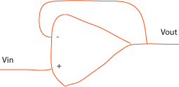
A basic operational amplifier (op amp) on an IC presents the designer with three pins:
IN+ , IN- , and OUT:

Inside the op amp IC is a differential amplifier with a large gain; the gain falls
off with increasing frequency of a sinusoidal input, but at "DC" the gain
is typically about 1^6.
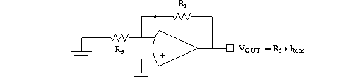
negative gain amplifier, 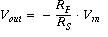
resistance can be replaced by the more general impedance of source and feedback
NOTES:
summing amplifier
current to voltage transformer.
op amp as a digital comparator
schmitt trigger with hysteresis
D-A converter
Positive gain:
high impedance UGFV
variable positive gain > 1
differential gain
combine both negative and positive configurations.
integrating amplifiers / low pass active filter
What is the input impedance of a UGVF? A*Rin
, huge!
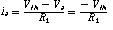
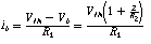
Showing that V- is virtual ground for negative gain configuration
Consider the op amp circuit below.
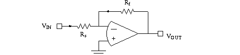
Note the current conventions on the diagram, and apply Kirchoff's current las
KCL to the V- node:
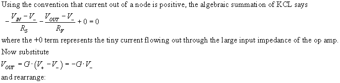
If Rf = 1000*Rs and G is 10^6, then Vin is in the range of 1mV, a so-called
virtual ground.
Almost no current flows into the op amp itself, because of the high input resistance
between V- and V+. Therefore only two terms appear in KCL, by algebraic summation.
[ Another derivation:
use Gs, Gf, and gain = A to see V- = Vin*(Gs/(A*Gf) ]
Therefore if G >> Rf/Rs then V- is very small-millivolts. And we would
expect that if Rf/Rs is not much much less than G then why not use the op amp
"open loop" circuit?
At any rate, remember that the gain of the negative gain summation amplifier is -Rf/Rs, a negative number.
Thinking about op amps and negative feedback diagrams
The analysis above suggests that the input stage is a voltage
to current converter, and the output feedback path is also a voltage-out to
current converter. The two currents add algebraically, and thanks to the negative
sign of the voltage-to-voltage gain, the sign of the feedback can be negative.
In that case the input and feedback pathways can be generalized to F(s) and
H(s) forms, while the internal path is G(s). The output can be seen as
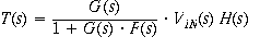
and it gives us an entry to study of op amp dynamics.
A summation amplifier: What is the result if TWO inputs converge on the KCL summation point at "virtual ground"?
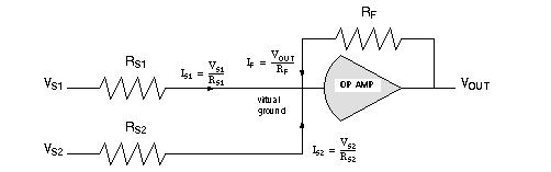
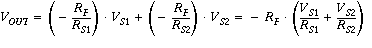
a negative gain summation amplifier that gives you the beginnings of a D-A converter, as discussed in the A-D lecture.
Input impedance and isolation
What is the input impedance of the negative gain
amplifier? Resistance is V/I. If the input is VIN, then the input current is
VIN / Rs, and therefore Rs is the input resistance.
It's not good that input impedance depends on a gain-setting resistor! It is
desirable that input impedance be large, but large value input resistors tend
to be susceptible to noise. Try the unity gain voltage follower (UGVF):
Compute the input resistance of the UGVF:
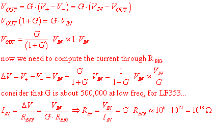
Such a large impedance isolates the input from
the output. RIN = VIN/I-IN; and I-IN is the current from the input through RBIG
to V- and V- is within G of VIN. So the input current is TINY.
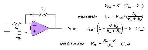
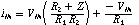
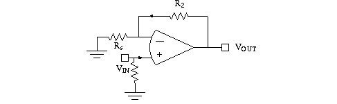
Try your hand at computing the gain of a positive input op amp circuit.
See circuit below. OK, gain is (R2 + RS)/RS ...
A UGVF results when RS = infinity and R2 = 0 (short circuit).
in the derivation below form Vout +V- = G*Vin ...
Sending a resistor from Vout to + input, can result in "negative" input resistance ...
See Roberge, p 457, for negative impedance circuit (NIC) below, and gyrator.
See diagram below.
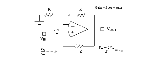
Using a NIC plus another op amp results in a gyrator--

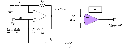
![]()
since 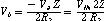
therefore

The wonderful result being that the impedance Z is now "inverted"; if Z were represented by a capacitor then the resulting input impedance would be mathematically identical to an inductor. The impedance would be from VIN to ground.
"Physical limitations of op-amps"
From Giorgio Rizzoni: Principles and Applications of Electrical Engineering, 2nd Edition, Irwin (1996). p. 575 ff
Clipping, from power supply limits;
Example of clipping from an integrator seeing offset.
frequency response, page 578, good plot for a practical op amp. Gain
shown as a ratio and in log form as decibels! And x-axis shown in radians/sec!
Looks like, open loop, the result of a low pass filter with 3dB cutoff w0, about 100 Hz!
One result, of a closed loop op amp circuit, is a fixed gain-bandwidth product. What is it
for the LF353? Looks like 4MHz. If gain is 100 then bandwidth limit is 40KHz, for example.
Op amp characteristics
There are three fundamental specs to consider: gain, bandwidth
and input impedance. Typical values for the LF353 IC amplifier
are shown below.
|
Basic Specifications |
Typical Values |
|
Open Loop DC Gain |
500,000 |
|
Gain Bandwidth Product limitation |
4 MHz |
|
Input impedance |
10^12 Ohms |
go to www.national.com to find LF353 website 2012: National acquired by TI: now list GBWP as 3MHz.
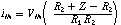
Input bias current. If the two inputs of an
op amp are connected together and placed in series with a sensitive ammeter
to ground, the resulting current is two times the input bias current.
Most common op amps, including the LF353, have junction field effect transistor
(JFET) on their inputs. What does the data sheet say the input bias current
is for the LF 353? 50 pico amps. In the LF353 the input acts as a source (current
flows out). Let's analyze the effect of input bias current on the output of
a negative gain op amp circuit.
Given the direction of the current, the output offset voltage will be positive.
Even if Rf is 100K, then the offset voltage is less than a microvolt!
Horowitz & Hill say bias current I_B is "half the sum of the input currents and the inputs tied together (the two input currents are approximately equal and are simply the base or gate currents of the input transistors)."
The transistor input stage may require or leak a little current
(going in or going out, more likely going out, "sourcing current"
as they say) and these bias currents can produce voltages across the gain setting
resistor, RS. One way to compensate for the input bias current: send a resistor
to ground that is equal to RS || RF
Input offset voltage. Even if the external input is zero, there may be a non-zero differential voltage on the input, that results in a non-zero output. You'll look for this offset in the Lab! You can tell about input offset only by measuring output. Therefore the output should increase as gain increases, in the absence of external input. What would it mean if the output were simply offset by a constant? Then it would be output offset voltage.
Slew rate limit. Consider at step change in input, and the expectation of a step change in output. The output will ramp up to the new value at the slew rate limit. It could be seen as a delay time through the chip, too.
Short circuit output current. (related to
output impedance). The load resistance to ground will compete with the feedback
pathway for current from the output source. The short circuit output current
is a rather crude way to think of the output impedance. How can you (in the
lab) measure output impedance? Find at what value of load resistance the unloaded
output drops in half (while taking into account the feedback path...).
Why doesn't the LF353 data sheet list a short circuit current
limit? What does it say about output short circuit?
On the LF 353 data sheet slew rate is 13v/msec
Log amplifier, Current-voltage for a diode, and temperature
sensitivity:
Current-voltage relationship for a diode is:
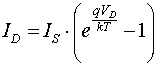
It goes through the point (0,0) on the graph! KT/q = VT ≈ 25mV. Where
saturation current IS is also a function of temperature T,
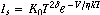
It is also known that I_S doubles every 5 deg C, so another way to say what
Is does is
![]()
I_s in the negative region of VD is small, about 10^-12
amps = pico-amp; see Chirlian, page 13.
Consider a p-n junction diode in the feedback path of an op
amp:
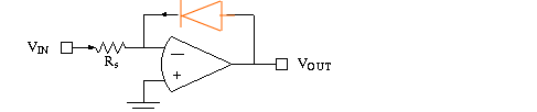
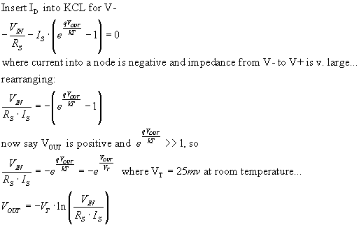
a logarithmic amplifier. The output is a compressesed version
of input.
And taking you back to your days of HS Algebra, what role
can logarithms play in multiplying two numbers together?
Now what about when VIN is positive, and drives VOUT negative? Then
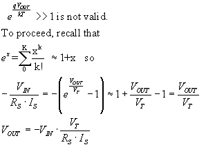
--a linear relationship on the other side of VIN
try graphing these two regions, to see a log compression effect !
Ideal op amp rectifier with diode. Think of the diode as a one-way wire: for positive V_diode the diode resistance is low; for negative V_diode the resistance is high.
See design below. Notice the arrangement is like a positive
gain circuit with R2 replaced by a diode, but with output in a different location.
When VIN > 0 volts the current can flow through the diode and does so until
VIN = VOUT. When VIN < 0 the op amp output saturates at the negative supply
voltage and the resistor "pulls down" VOUT until it's zero.
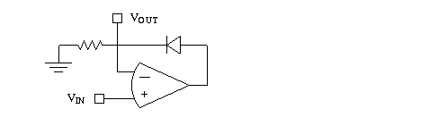
No current flows through the diode when VIN < 0; therefore VOUT will be 0.
If you graph VOUT vs VIN you will see the relationship for a half wave rectifier.
There is no 0.6 v threshold: the
op amp turns a diode with a nonlinear I-V curve into a perfect rectifier.
Capacitor in the feedback loop
Op Amp Integrator. What if an ideal capacitor takes up the feedback
path?
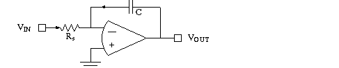
Use Laplace transform to find the (gain) transfer function, ZF / ZS
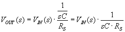
What operation is associated with 1/s? (to get us back to the time domain).
Integration! (The Laplace transform of step function is also 1/s...)
If a resistor were in parallel with the capacitor a leaky
integrator (LP filter) would be in the feedback pathway.
One op amp configured as a differential ampler with adjustable
gain
"True" Differential Amplifier with one op amp:
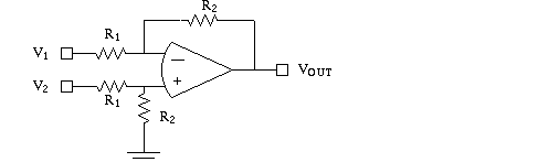
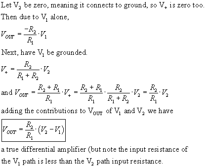
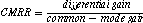
The extent to which the above formula is NOT true is expressed by the common mode rejection ratio, in log dB, as the ratio of common mode to differential mode gain. Thus CMRR will be a negative number, in dB. The CMRR of the circuit above will not be good if 5% tolerance resistors are used.
The common mode gain is the gain (or more likely, attenuation) at the output when
both differential inputs are set to the same value, say 10 volts. If for example both inputs at
10 volts results in an output of 0.01 volts = 10 mV, then the common mode gain is
.01/10 = .001 = -60dB. If the differential mode gain of the same circuit is, say, 1000 = +60dB
then the CMRR is .001/1000 = -120 dB
OP AMP SPECs
SEE 353 DATA SHEETS
* OFFSET INPUT, OUTPUT
* GAIN BANDWIDTH PRODUCT
GAIN AT 1 HZ
* Input noise.
* Input bias current
* Common Mode Rejection Ratio
MEASURED IN dB.
* Settling time & rise time to a step response
Offset to zero by op amp or by Wheatstone bridge:
To give the smallest "background" voltage input
to an amplifier, place a resistive sensor in a Wheatstone bridge: The output
will "float", and should be amplified by a true differential amp (instrumentation
amp).
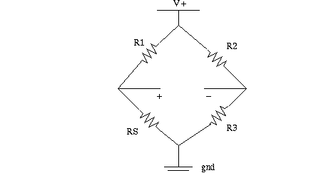
What happens for different placements in the bridge? what if a "dummy sensor"
is placed in another leg, can temperature or other factors be compensated? Or
will the gain double, in the case of the thermistor Lab 5? You'll learn more
when we get to strain gauge lecture notes.
Instrumentation amplifier
Has true differential input and a gain which can be set accurately and independent
of input circuits. See AD524 Data sheets.
Imagine UGVFs on both inputs to a differential op amp configuration. With trimmed
resistors to minimize CMRR.
gain is constant over a wider frequency range
excellent CMRR, which is
measured in decibels
Derenzo, page 56, "While many of the previously discussed op amp circuits
have constant gain, one must choose between high input impedance and differential
amplification. The instrumentation amplifier provides both properties."
See 524 website for more spec on the inst. amp used in the lab.
Isolation amplifier
Methods of isolating:
UGVF
convert electrical to LED transmission, photox reception
transformer
wireless: Bluetooth, WiFi, radio
the role of voltage-frequency converters...
Isolation amplifier AD202, from Analog Devices.
go to website http://www.analog.com
IA has physical separation of input from output.
optical, transformer methods.
Necessary in some biomedical applications, for patient safety.
Sacrifice: gain-bandwidth is much less, in the KHz range.
Summary
* Operational Amplifiers:
negative gain summation configuration
positive gain high input impedance
* Instrumentation Amplifiers
more expensive, and custom made for excellent common mode rejection ratio,
with high input impedance. fixed choice in gain. Better gain-bandwidth product
* Isolation Amplifiers
yet another step up in cost, for "physical" isolation of input from the rest of the
circuit. Useful in biomedical applications, for patient safely. Isolation by optical, or
inductive means.
*
![[ Another derivation: use Gs, Gf, and gain = A to see V- = Vin*(Gs/(A*Gf) ]](../eqnAMP/KCL_opampGA.gif)