Successive Approximation Design Example
1: In a 4-bit SA conversion,
SOC always activates the same first guess: 1 0 0 0 = 8-base10. This guess is halfway
up the range of possible answers the system can consider:
1 0 0 0 goes to the DAC, which converts it to an analog voltage to be compared
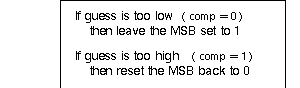
with the unknown analog input. If the converted 1 0 0 0 guess is greater than
the unknown, then the comparator will put out a "1". This comparator output
goes back into the S-A circuit and inside the following rule is used:
With the MSB decided, the sequence of successive approximations is started and the
next guess focuses on the 2nd MSB. The second MSB is set to 1 and a new DAC output
is compared with the unknown analog in. The rule stated in the box above is now
applied to the 2nd MSB.
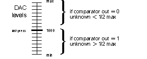
As an example, imagine that max = 8v, min = 0 v and the unknown
= 5.75 v. The first guess (1 0 0 0) results in a DAC output of 4.0 volts and
a comparator value of 0. The MSB stays set at 1. The next guess is 1 1 0 0,
with a DAC output of 6.0 volts. The comparator value is 1, so the second bit
is reset and the third guess becomes 1 0 1 0. This third guess results in DACout
of 5 volts, comparator out of 0 v. and no reset of the third bit. After a fourth
cycle of narrowing down the range, a final answer of 1 0 1 0 is achieved.
A "20 questions" yes-no process continues down from the MSB to the LSB at which
point conversion is complete. Note that an 8-bit conversion should take only 8 cycles,
instead of the maximum 256 cycles in a plain ol' counting converter. What happens at the
end of conversion? The S-A circuit knows it has reached the LSB and sends out an
EOC pulse, so the answer can be latched for display or placed in memory.
2. Inside the S-A circuit
Let's look at what must be inside the S-A circuit.
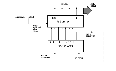
The guesser can be divided into a set of latches (the SA register) and a sequencer.
We will consider the sequencer in detail later; for now assume its outputs a-h are
high (active) one at time, in sequence (a shift register is involved...). For continuous
converting we have shown the EOC output connected to the SOC input.
The SA register is a group of Set-Reset latches:
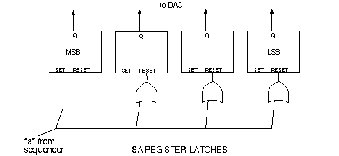
The first pulse in the sequence, a, SET's the MSB and
resets the other bits, to establish the guess 1 0 0 0. The next control pulse from
the sequencer, b, is AND'd with the comparator feedback: If both are true
the MSB latch is reset back to 0.
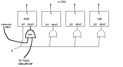
The 3rd control pulse, c, SET's the 2nd MSB latch to
provide the next guess.
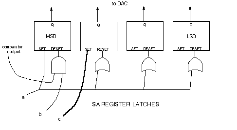
And, like before, if the comparator returns a value of 1, the
2nd latch is reset (because the guess was too high).
Consider whether it would be possible for one pulse to do the work of pulses b &
c, that is, have the reset of MSB latch occur at the "same time" as the
set for the 2nd MSB. Observe that there is a gate's worth of delay to reset, and
no delay to set, so set may occur before reset, resulting in a "timing
error," or improper DAC-guess being generated.
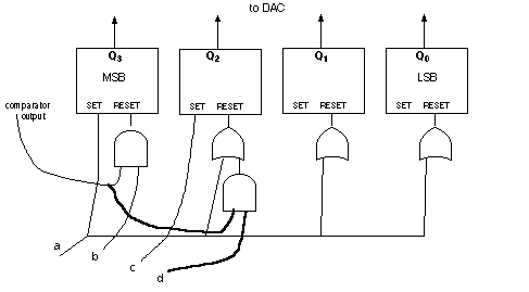
The SETing and possible RESETing of latches continues on down
the line until the last bit is decided. Note that on the last cycle the complement
of the comparator itself has the value required for the LSB:
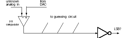
Can you get away with no latch for the LSB?
Probably not...at some point the LSB must be set as part of the last guess...
3. The sequencer
Let's see what the timing diagram looks like for the
sequencer output; you can see these waveforms on the logic analyzer if you like:
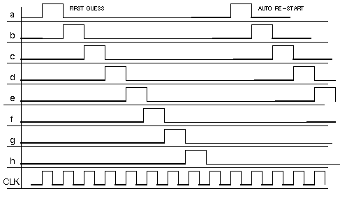
These are the waveforms of a serial shift register, shifting a solitary "1"
to the right, then cycling the "1" back to the start:
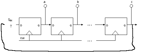
The 74164 serial in-parallel out shift register can do the job of shifting, but
if you simply hook up the last flip flop output Q with SIN, you'll have problems:
How do you get it to start up properly? What if it drops a bit, or if the sequence
picks an extra 1...how can mistakes be corrected?
Consider the circumstances under which you want a 1 returned to
Sin-there are only two cases (if we're dealing with all 8 sequencer outputs):
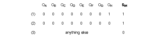
The all-zero condition corrects for bit-dropping or startup problems. Ironically
enough, this truth table shows that QH, the last stage output, is a don't
care. All that matters is whether the other bits are zero. What logic operation
returns a 1 for all zero inputs, and a 0 for anything else? If
you're thinking it's an OR gate, you're wrong, but you're close... Once
you insert such a logic gate on the input SIN, and hook up the sequencer outputs
to the SA register set, you're (essentially) done with the "internal"
part of the SA design.
4. End-of-Conversion
The end-of-the-line pulse from the sequencer can latch the answer from the SA
register into a set of latches which lead to the display. By this means the display will be
updated only when a new answer occurs; other states of the SA register = S-A
circuit will be ignored by the display. When troubleshooting you may want to bypass
the latch and show directly the SA register state. Notice that SA will always find an
answer, even if AIN > DACMAX; in which case the answer will be 1111. Recall that the
counting converter would make a mistake for AIN > DACMAX, because the DAC couldn't
generate a value large enough to trip a comparator.
Need for constant value during conversion. Look what
would happen if the unknown analog input decreased from, say, a value above 1/2
max to a value below 1/2 maxafter the MSB had been set: A wrong answer
would result because all the subsequent bits reset to 0. Then again, what is being
converted if the AIN(t) is allowed to change during the conversion process? Here
we're just repeating the need for sample-and-hold in a high speed converter system.
In the SA example, the potentiometer knob is turned so slowly that changing input
is not a problem.
Consider a CHIP LIKE THE 74LS502, "8-BIT
SUCCESSIVE APPROXIMATION REGISTER".
A CLOCK + 'LS502 + DAC + ANALOG COMPARATOR CAN BE A COMPLETE a/d CONVERTER.
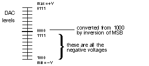
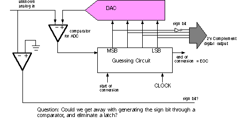
3b. Converting negative voltages
to 2's complement digital form
Assume analog input can be in the range +/-V. First let's modify
our DAC so it puts out voltages in the range -V to +V:
In addition to this adjustment, we need to invert the MSB answer bit. Notice
that this scheme looks different from the invert-&-add-1 algorithm usually seen
with 2's complement. See diagram below-
NOTES...Consider DAC by R-2R alone...use AD7524
5. Sample & hold and analog
switches
Consider what a sample-and-hold and analog switch might look like
and do. A sample and hold can be designed as:
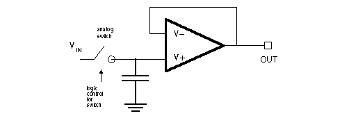
When the switch is closed (sample) the circuit functions as a UGVF; the high input
impedance of the UGVF insures that the capacitor doesn't filter too many high frequencies.
MORE: "Hold" means remember, remember an analog number, for, say, less
than a second. Our only analog memory element is a capacitor, so let's charge a capacitor
with Vin(t) and hope it holds...
We'll use our new best friend the analog switch to go from
sample to hold mode. When Vin(t) is disconnected from from the capacitor we
don't want it to leak off its charge; thus the UGVF with huge input Ω
comes in handy (we also hope the analog switch, when in the OFF position, has
an equally huge input Ω). There is a trade-off here. To sample rapid changes
in Ain(t), we want capacitor C to be as small as possible; to hold without droop,
we want C to be as large as possible.