Frequently Asked Questions
Please check here first to see if your question has already come up before. Below are some answers to frequently asked questions.
-----------------------------------------------------------------------------------------------------------------------------------------------
When I try to edit the schematic of my gates, Cadence gives me the following response window:
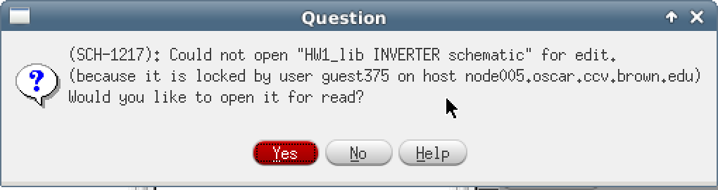
What should I do to edit the gates?
The solution is to run the following command from the terminal:
rm ~/Library_name/Cell_name/schematic/*cdslck*
where Library_name and Cell_name need to be replaced with the names from the library manager.
-----------------------------------------------------------------------------------------------------------------------------------------------
How do I zoom in to see details of my simulation waveforms?
Double-click on the x axis and in the "Scale" tab, select Manual mode and set the Minimum and Maximum axis limits.
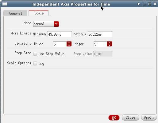
In particular, you may find it useful to zoom around the transition of signal with a range comparable to the rise/fall time of an imput signal.
-----------------------------------------------------------------------------------------------------------------------------------------------
What should I send as part of my DRC and LVS runs?
Both DRC and LVS generate a report file (cell_name.drc.summary and cell_name.lvs.report respectively). It will be enough if you send these files to the TA.
-----------------------------------------------------------------------------------------------------------------------------------------------
How do I transfer files from the CCV server to my own machine?
There are several ways to do this:
- Launch Firefox (installed on the CCV machines) and access your Brown mail account. From there you can send email to yourself with the appropriate files attached.
- Use the scp protocol. If your machine runs OS X or Linux you can run the command from terminal ('man scp' will give you the usage details).
- On a Windows machine, you can use the WINSCP application to transfer files.
-----------------------------------------------------------------------------------------------------------------------------------------------
How do I determine transistor sizes from the effective fanout and gate capacitance values obtained from computing logical effort?
Using the example from Lecture 11 on path delay (see circuit on pages 3-4 of the lecture slides):
- We found that the gate effort h=1.93 for all gates in the path. Note that h=figibi.
- We then calculated f4 = 1.93, f3 = 1.16, f2 = 1.16, f1 = 1.93. Using the definition of fi = cg,i+1/cg,i we calculate the gate capacitances working backwards and got: cg,4 = 5/1.93 = 2.59, cg,3 = 2.59/1.16 = 2.23, cg,2 = 2.23/1.16 = 1.93, cg,1 = 1.93/1.93 = 1.00.
- We can then use these gate capacitance values to figure out the actual size of the gates. Note that cg,1 = 1 is given in terms of a minimum sized inverter so all subsequent gate sizes are relative to this. So again if we work backwards we see that gate c is 2.56X the size of a minimum sized inverter. Since gate c is also an inverter, we determine that it should be scaled up to be 2.56 times as large as the first inverter in the path.
- For gate b we found that it is 2.23X the size of a minumu sized inverter. A minimum sized NOR2 is 5/3 as big as a minimum sized inverter so gate b should be scaled up by 2.23/(5/3) = 1.34 (i.e., gate b should be 1.34 times as large as a minimum sized NOR2).
- For gate a we found that it is 1.93X the size of a minimum sized inverter. A minimum sized NAND3 is 5/3 as big as a minimum sized inverter so gate a should be scaled up by 1.93/(5/3) = 1.16 (i.e., gate a should be 1.16 times as large as a minium sized NAND3).
-----------------------------------------------------------------------------------------------------------------------------------------------
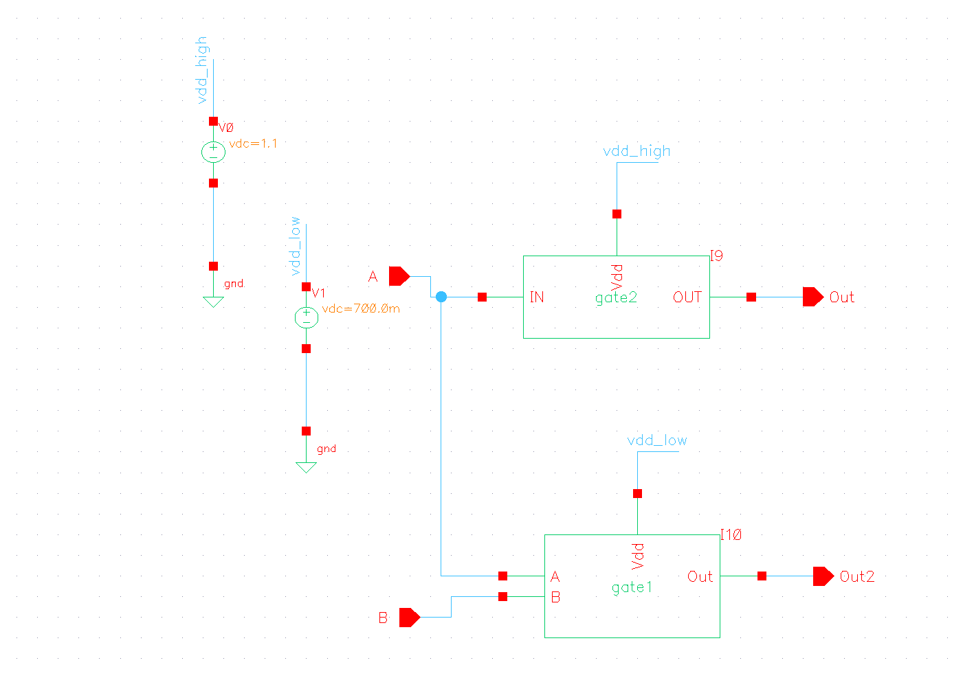
How do I set up a simulation in Cadence to handle multiple Vdd values?
In earlier homework assignments, we have used 'vdd' and 'gnd' instnces from the analogLib library for connecting the power supply nodes. These work as global node connections since they are implicitly visible to all gates throughout the design hierarchy.
If we need to specify different values for Vdd, we need to make the Vdd connections accessible from outside the symbol view of the cell. This can be done by replacing the 'bdd' symbol from the analogLib with an inputOutput pin.
When designing the top view cell, we can make a connection with the proper vdd source by using wire lables (pressing 'L'). the figure below shows how gate2 is connected to vdd_high while gate1 is connected to vdd_low.
-----------------------------------------------------------------------------------------------------------------------------------------------
How can I share files in Cadence in order to work on a group project together?
Create a folder in the data path of the class group and copy the project files there.
I now have the shared folder, but I no longer have access to my library.
How can I fix this?
You have to create the library from scratch but point to the path where the files are saved.
-----------------------------------------------------------------------------------------------------------------------------------------------
When I run the PEX extraction of my layout, I get thousands of warnings and errors. When I look at the PEX output schematic
it seems like some of the pins of the transistors are overlapping. Is this normal?
There is an option in the Calibre view setup that should solve the problem. Before running PEX, go to Calibre -> Setup -> Calibre
view and towards the bottom of the window check the option Device placement: Arrayed.
This should give a more regular placement of the instances.
-----------------------------------------------------------------------------------------------------------------------------------------------
Back to ENGN1600 Home page