(a) What signal should control the clock on the RR register?
(b) What should be the microprogram instructions, bit for bit, for JSR and RTS, the jump to and return from subroutine? Assume there is a FE line from microcode.
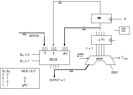
1. Here's a diagram for hardware which will store the return address for a jump into a RR
register, for later recall on a RTS (return from subroutine) instruction.
(a) What signal should control the clock on the RR register?
(b) What should be the microprogram instructions, bit for bit, for JSR and RTS, the jump
to and return from subroutine? Assume there is a FE line from microcode.
2. A real 2901 processor chip has 5 inputs to its 2-output SOURCE MUX. (a) How many bits of selection are required to account for all of the combinations of 5 things taken 2 at a time? (b) To what does the answer increase if it matters which ALU input port an input goes to? (Calculate the number of permutations of 5 things taken 2 at a time ... Q, D not the same as D, Q)
3. Show a circumstance (SFD) in which data races around the 2901 if latches are missing from output of the RAM.
4. What do think is the closest analogy for: Microprogram is to computer as
(a) chocolate chips are to cookies
(b) carburetor is to automobile engine
(c) index is to book
(d) software is to hardware
5. In the first stages of address generator design we consider two alternatives for the CONTINUE option: (i) an up-counter driven by the system clock or (ii) a combinational incrementer feeding a register which in turn is one selection of a MUX whose output is the current address. Your question: which of these two alternatives is faster? Find a TTL data book (or data sheets of JD Lab Manual +) and look at propagation delays of a counter like the 74169, a register like the 74174, and a MUX like the 74151. What is the total propagation delay, in nanoseconds, for each of the two designs from rising edge of clock to new address, Y+1?
6. Suppose a CONT instruction is imposed on a microprogram sequencer, and carry-in of the incrementer is set to LO. What will happen at the output?
7. How could the "next address" part of microcode, which projects back the the address generator of the microprogramming control unit, be used to eliminate the need for the "continue" pathway into the address generator MUX? What cost would be involved in having the next address feature take over the "continue" function? Specifically, how would JSR work with the "continue-less" approach?
8. Can you design an address generator with CONTINUE and JUMP features, using an up-counter with load, instead of an incrementer and a MUX?
9. There is a "timing problem" with the following attempt at one-level subroutining
What is it? [Hint: Consider what does happen and what should happen on RTS, return from
subroutine. What's going on with USR CLK? Why is it needed for JSR?]
10. LIFO stack timing during JSR. Here is a sequence of events for one JSR, where M is the main memory address at which we leave for the subroutine-(1) INC-reg latches M+1 (2) stack pointer is incremented (3) M+1 is written into stack. Show on a timing diagram how system clock & instructions bits for JSR (SE, PUSH) should be sent to the INC-reg clock, the stack pointer counter, and write-enable of the stack.
11. What is on the stack output during RTS? Consider the timing waveforms below, for a
sequence of JSR, CONT, & RTS instructions to a microprogram sequencer capable of
nesting subroutines. The stack pointer clock is falling edge triggered. The main memory
location of the JSR is M, and the first subroutine address is S. In small numbers along with
the SE�CLK waveform is the current address of the stack pointer. Assume that PUSH/POP
drives a level-sensitive write-enable on the memory stack.
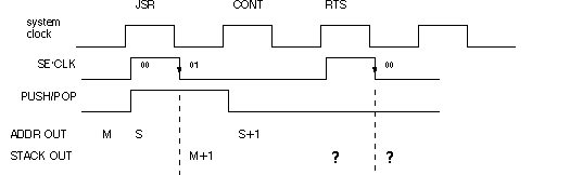
(a) What the address output and the stack output at the times of the question marks?
(b) What would be ADDR OUT if two JSR's were followed by two RTS's?
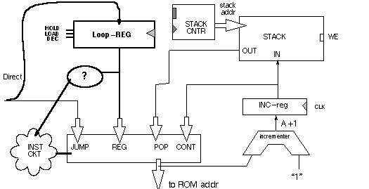
12. Loop counter. The 2910 sequencer has a loop register which can be loaded from the DATA
bus. The register can be LOADed, HELD, or decremented. The loop-register serves two
purposes: (1) If HELD and selected by the MUX, it can be an internally-saved address (2)
If decremented, it can be used to count how many times an instruction in the JUMP or FILE
addresses is repeated.
Your questions: What should go in the box marked with ? in the diagram below?
How should the result of the ? oval be used by the instruction decoder in the the cloud at
the lower left?
For more information consult the 2910 data sheet.
13. An instruction set for a sequencer. Assume you have 3 instruction bits, I2. I1, I0 , and one
FAIL bit as inputs to the sequencer. Outputs need to control MUX SEL with CONT, POP and
JUMP mux inputs, and output enables for PL (pipeline), MAP and VECT. A 4-deep stack
has requirements for CLEAR, SE (stack enable), PUSH & POP. Here's the instruction set:
I2. I1, I0 PASS FAIL
0 0 0 INIT (clear stack) --
0 0 1 CONT JUMP TO PL
0 1 0 JUMP to PL --
0 1 1 JUMP to VECT --
1 0 0 JUMP to MAP JUMP to VECT
1 0 1 JSR (jump to subroutine) JUMP to PL
1 1 0 RTS (return from subroutine) --
1 1 1 REPT (the previous inst) JUMP to PL
Design a combinational circuit to implement this instruction set.
14. Timing for nested subroutines. Suppose three JSR instructions in a row are sent to a
microprogram sequencer. The system clock and the JSR signal may look like,
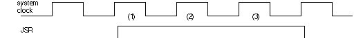
The JSR signal has only one rising edge. How can the sequencer know that three separate JSR's occurred?
Will there be another problem if JSR goes directly to write-enable (WE) of the STACK RAM and the WE is a level-sensitive input?
15. You are given a microprogram sequencer with the following "instruction set".
S1 S0 FE PUP
CONT= continue by increment 0 0 1 1
JUMP to D bus address 1 1 1 0
JSR = jump to subroutine 1 1 0 1
RTS = return from subroutine 1 0 0 0
JPP = jump & pop 1 1 0 0
where S1 and S0 are MUX selects, FE is file-enable (active low) for a 5-deep stack, and
"PUP" is a push-pop signal. JPP jumps to the D-address and pops the stack.
What sequence will be generated by the following program for a 5-bit address?
inst D-value
JUMP 0
JUMP 4
JUMP F
CONT 0
CONT 0
JUMP 6
CONT 0
JSR 1
RTS 0
JSR 2
JSR 6
JSR A
CONT 0
RTS 0
RTS 0
RTS 0
JSR 3
JPP 0
16. Suppose an 8-bit CPU is required to address 64K main memory locations. Think of an arrangement of memory address register(s) to accomplish this. Imagine that the main memory is composed of eight 64K dynamic RAM chips, which need to receive row, then column, addresses, as we saw in the chapter on Memory.
17. (a) What might go wrong if there were no Memory Address Register, and the CPU tried to
address main memory with the output of the shifter? The CPU could still keep track of the
program and data pointers in its cache memory, but ...
(b) Could the MAR be "replaced" by registers in front of the mapping ROM and the DATA
input of the ALU MUX?
(c) What might go wrong if there were no Memory Data Register, and the shifter were tied
to the memory data bus through a 3-state buffer?
18. Following the example in the text,
(a) List in RTL the sequence of actions required microcode to accomplish a "SUBTRACT
RAM from ACC" user instruction. Assume the cache memory in the CPU contains a
program counter, a data pointer and the current value of ACC.
(b) List the microcode actions needed to store a word in main memory that is currently
in an register "TEMP" near the ALU.
19. RISC=Reduced Instruction Set Computers have been implemented in various forms in
commercial hardware, most notably at Hewlett Packard. From what you've learned in this
� you should be able to appreciate that RISC machines arrange one machine cycle per
user instruction. By that means, one wouldn't have to design in all the next-instruction,
next-jump features in the microcode of the machine designed in � 17. RISC can even
mean fewer than 1 cycle per instruction. IBM claims that five instructions per cycle can
be carried out in their RS-6000 workstation!
Speculate how a machine could be designed which could do more than one user
instruction per clock cycle.