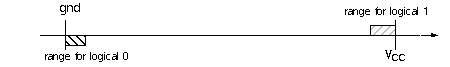
(b) What disadvantage would accure from restricting the logic ranges to the far corners of the possible voltage range of the chip?
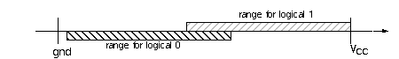
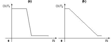
1. (a) Is it ever possible for the voltage ranges of logical 0 and logical 1 to overlap, as shown
below?
(b) What disadvantage would accure from restricting the logic ranges to the far corners of
the possible voltage range of the chip?
2. A weak binary signal B between 0 and 2 volts must be boosted by a factor of two before its
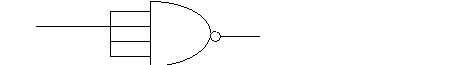
HI value can cross the threshold of an inverter and OR gate shown below.
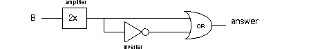
(a) What is the answer of the circuit? Say it out loud. "Two B..."
[Hint: Who said, "There are more things between heaven and earth Horatio, than are dreamt of in your
philosophy." ? Thanks to S. Derman, IEEE Trans. on Educ. 34: #4 (1991)]
(b) Due to non-zero propagation delay through the inverter is there any time during
switching of B when the answer is only "to be"?!
3. Consider the linear inverter described in the first part of �8, where OUT = 5 - IN over the
range 0 < IN < 5. What does OUT look like, as a function of IN, if we say that
0 < OUT < 5 (a saturation condition) and OUT = (2.5 - IN)�10 (gain of 10)?
4. Draw the IN-OUT curve for the 3v inverter circuit shown below
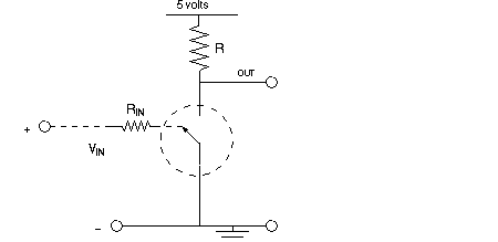
5. The inverter gate below includes a RIN on the control voltage path of the switch. RIN models
the input resistance of the gate, which in the case of a TTL gate is actually the base-emitter
junction of a npn transistor. If R=1000W and if RIN=100W what are (a) the maximum current
which can be sent out of OUT and (b) the droop in OUT if a gate at a HI level is connected
to another gate with RIN ?
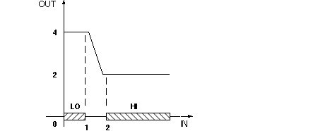
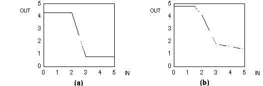
6. For the logic levels defined on the input axis below, will the curve shown work as an inverter
capable of driving another inverter like itself? Assume input resistance of the gate is much
much greater than output resistance (max OUT won't change upon loading).
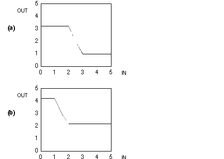
7. Will chips with the following input-output characteristics be able to act as functional
inverters when an odd number are connected end to end?
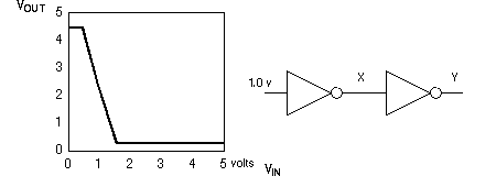
8. Below is shown an asymmetric I-O curve. It is used in the inverter pair shown on the right.
(a) What are the values of X and Y if an input = 1.0 volts for the circuit on the right?
(b) Can a gate with the I-O curve shown function as an inverter?
(c) Is there any value on the curve where VIN = VOUT?
9. The two inverters curves shown below have the same maximum and minimum output
voltages. Which is to be preferred for use in switching circuits, and why?
10. Imagine a voltage-controlled switch with a control voltage which can be preset between
0 and 5, and a maximum allowed current through the switch of 100 mA. Suppose you are
required to design the switch into an inverter gate which will deliver no more than 50 mA
of current and which will have a voltage range for LO less than 1.0 volts, and a range for
HI greater than 3.0 volts. (a) Draw out a design for the inverter gate, using a resistor of
minimum size, and a power supply of +5 volts. What should the preset control threshold
be?
(b) Will your inverter gate be capable of driving another gate like itself?
(c) Suppose the control input sinks 5 mA of current when its voltage is 3.0 v. What will be
the fanout of your inverter gate?
11. Another way to look at input-output matching. Find a clear plastic sheet (like the kind used for viewgraphs). Trace each of the two curves shown in problem 6. For each curve turn the sheet over, rotate it 90� and superimpose it on its starting curve. How many stable solutions (intersections) exist for each of the two curves given?
12. Draw an inverter curve for a chip in which VOH-min = VIL-max .
13. (a) What are VOH, VOL, VIH, and VIL for the inverter I/O curves shown below?
(b) What are the noise margins for the two curves?
14. Compared to the formulas for noise margin in the text, what would be an advantage and
a disadvantage of using the following primed formulas for noise margins?
DVL'= VIL - VOL.
DVH'= VOH - VIH.
Draw out a typical inverter curve and show as horizontal bars where these noise margins
would appear.
15. What are the noise margins DVL and DVH for each of the following 4 inverters?
16. Find the best match for the following analogy: Noise margin is to voltage parameters as
(a) Speed limit is to horsepower
(b) Discount is to price
(c) remainder is to quotient
(d) area is to radius
(e) orbit is to gravity
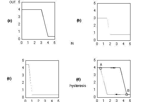
17. The data sheet for a 7414 TTL hex Schmitt-trigger inverter chip lists two parameters, VT+
and VT-, positive-going and negative-going thresholds.
VT+ = 1.7 volts
VT- = 0.9 volts.
(a) If VOH = 3.4 v and VOL = 0.2 v, then draw a graph of of what you expect input voltage
vs output voltage to look like. [Hint: think hysteresis]
(b) What are the high and low level noise margins for the 7414?
18. Possible TTL and CMOS voltage parameters are given below:
TTL CMOS
VIL 0.8 1.4
VIH 2.0 3.9
VOL 0.4 0.2
VOH 2.4 4.0
For this question ignore current output limitations. (a) Can a TTL gate drive a CMOS gate,
or does it need a level shifter? (b) Can a CMOS inverter drive a TTL inverter?
19. What would be wrong with making sure an used TTL input was always HI by connecting it +8 volts?
20. In �1 you saw circuits for diode logic. A formula was given for current flow through a diode. To the extent that a gate input acts like a diode, what do you expect to happen to current parameters as temperature increases?
21. The data sheet for the 7414 chip lists the following parameters:
IOL 16 mA
IOH -800 mA
IIL -0.8 mA
IIH 40 mA
What is the worst case fan out?
22. CMOS fanout. The data sheet for a certain CMOS chip (74C04 inverter) list the following
static parameters for each gate on the chip :
IOL 0.025 mA
IOH -0.25 mA
IIL 0.5 mA
IIH -0.5 mA
(a) What is the worst case static fan out?
(b) Will dynamic fanout of CMOS be greater or less than static fanout?
23. Presuming noise margin problems with voltage parameters are not an issue,
(a) How many 7414 inverters can one 74C04 inverter fan out to, given the data in the
previous two problems?
(b) How many 74C04 inverters can one 7414 inverter fan out to, given the data in the
previous two problems?
24. If an output must project to 100 other gates but is rated for only a fanout of 9, extra
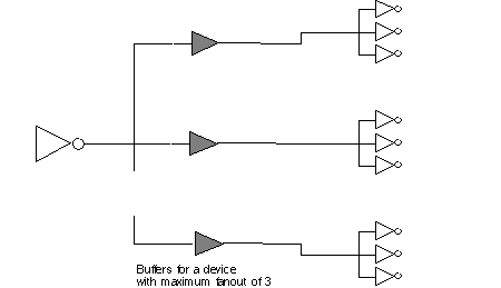
(non-inverting buffers) will be needed to make the design viable. Assume the buffers have
fanout of 9 also. (a) How much extra delay is caused when a chip is limited to fanout of
9 but must project to 99 other gates? Assume each gate has tpd propagation delay.
(b) What is the extra delay when the fanout of the chips is limited to 3, but 99 must be
driven?
25. Suppose a 4-input TTL NAND gate has all 4 inputs tied together.
Does it represent 4 gates worth of fanout load, or one? It will matter whether you consider
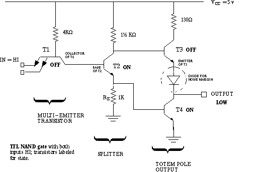
the high level or low level fanout. Look at the diagram of the "classical" TTL gate at the end
of �9, or study a TTL gate input in a TTL data book. Try to follow where current would flow
in both high and low level cases.
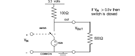
26. Consider a load in the form of a resistance to the +5 rail. (a) If the switch on the inverter
gate shown below is closed, how much current IL flows in to the gate? (b) What is the total
current which flows through RE in that case? (c) If RE = 3W and RC = 1000W and
RL = 100W and VOUT must stay below 1v for logical LO, then how many loads can the can
fan out to before VOUT goes above 1v?
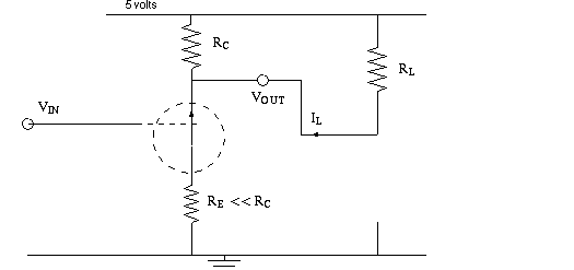
In an actual TTL or CMOS gate the output resistors RC and RE are replaced by transistors.
27. Open collector logic: What is the Boolean expression for two 3-input open collector NOR gates tied to the same pull-up resistor? Let the inputs be A-F.
28. Wired-AND. When N open collector inverter outputs are connected to the same pull-up resistor, an N-input NOR gate results. This is sometimes call a "wired-AND" gate because all gates must be active for the output to change. Re-draw an N-input NOR gate as an AND gate with inverters.
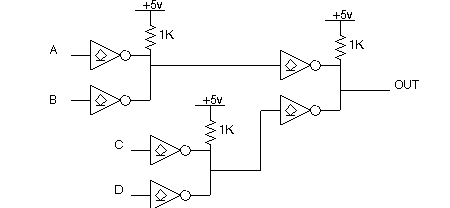
29. What 4-input, 1-output logic expression is realized by the following arrangement of six
open-collector inverters? There are six OC inverters in a 7406 chip.
30. The 7406 open collector inverter data sheet lists the maximum allowable current through
the gate at 40 mA. Assume a 7406 inverter is to drive 3 TTL gates, each of which may deliver
IIL of -1.6mA.
(a) For pull up to 5v what is the minimum sized pull-up resistor that can be used?
(b) Now consider current which passes through RPU when the 7406 output is held HI.
Assume IIH of 40mA on each of the 3 gates fanned out to. And when the transistor in the
7406 inverter itself is OFF 200mA of current leaks through it to ground. Furthermore, VOUT
for the 7406 when output is HI must be greater than 2.0 volts for our definition of logical
HI. What is the maximum sized pull-up resistor that can be used?
[Hint: A 1KW resistor will fall in the range between min and max for the pull-up resistor.]
31. Draw the design for a 4!1 non-inverting MUX, using open-collector NAND gates.
32. Without an output pull up resistor a 7406 open-collector inverter is able to drive properly a 7414 inverter, but is not able to drive a 74C04 CMOS inverter. Why? Hint: Think about what's on the input of each chip.
*33. Transistor as an inverter. The relationship between collector current, base current and
the voltage between collector and emitter is condensed into the set of graphs shown
below, for an npn transistor. For the circuit shown on the right the transistor operating
curves must intersect the diagonal load line with slope 1/R
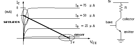
If the collector-to-emitter voltage is the output of the transistor, in which region of the
curves shown is logical HI represented? Logical LO ?
*34. In what way is a totem pole output like a real Indian totem pole? What advantage(s) does
a totem pole output have over a single npn transistor output, shown below?
35. Darlington output. Suppose the linear current gain of an npn transistor, IC/IB , is hFE.
If two npn transistors are connected as shown on the left below, as a Darlington pair, then
the overall linear current gain, from IB1 to IC2 , is the square of hFE.
Most modern TTL chips (LS, F, ALS sub-families) have Darlington outputs. An example
of a Darlington output for a TTL gate is shown on the right of the diagram below.
In some logic families Q1, Q3 and Q4 are Schottky transistors.
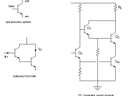
(a) In the diagram above, on the right, which transistors make up the Darlington pair?
(b) If RL is smaller, then the transistor switches more quickly. Why? [Hint think about RxC]
(c) The increased current from a Darlington pair improves fanout. Which fanout,
high-level or low-level, is most improved by the Darlington pair?
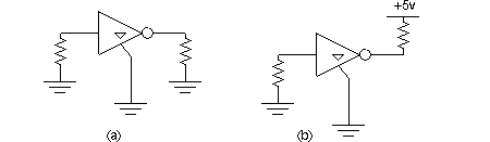
36. Three-state output analysis. What do you expect the output of the disabled 3-state
gates shown below to be? All resistors are 100W.
37. Bidirectional transciever designed with 3-state outputs. Suppose two points, "left"
and "right," are to be connected through a box

When direction control is HI, data can move from left to right; when direction control is LO
data moves from right to left. Design the insides of the box, using 3-state gates.
38. The 20-pin 74LS240 3-state inverter chip has 8 inverters in two groups, A and B; each
group has a separate enable pin. See logic diagram below. Power and ground pins not
shown. Pins GA and GA are the active-low gate enables for groups A and B.
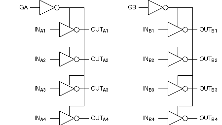
Show how, with the help of one more inverter, the 74LS240 can be configured as a quad
2!1 inverting MUX.
39. The 74F125 3-state quad inverting buffer lists IOHZ = 50 mA and IOLZ = -50 mA in its data
sheets. Does a disabled 74F125 have enough current capability to fan out if
| IIH | =| IIL |= 20 mA?
When could fanning out from a disabled 3-state output make sense?