S2 Speed & Power in Logic Families
--------
Link to End of chapter Exercises:
The previous Supplemental Chapter dealt with static parameters ("DC
characteristics") of voltage and current for digital chips. This chapter on dynamic
parameters extends our look at data sheets to what are called "AC
characteristics"-various propagation delays and timing requirements. We also look at the
relationship between power consumption and switching speed. In the process it is
necessary to compare various semiconductor versions of logic gates. The marketplace
has provided an environment for a struggle between different versions of logic chips. Over
the years some logic families have survived the struggle and thrived, while others have
become virtually extinct. In this chapter we examine the surviving families, and study their
evolution. We see what virtues the survivors possess-chief among these are fast
switching speed, low power consumption, high packing density and reasonable cost per
gate. To proceed, you may want to review facts of electric circuits with energy-storing
capacitors-including what an RC time constant is.
S2 / 1 The virtue of speed
Back in 1987 an IBM RT workstation could load my desktop publishing program
INTERLEAF from hard disk to main memory in 40 seconds. After a central processing
unit (CPU) upgrade in 1988 the RT could load the same benchmark program in 30
seconds. Why the reduction in loading time? The hard disk hadn't been changed, so
the reduction must have come from improvements in the CPU. While there may have
been some advances in the CPU's "architecture"-notably more parallel processing
and better direct memory access (DMA)-a major improvement was in the shorter
propagation delays of individual gates and chips. Faster hardware is better, all other
things being equal. We'll see in this chpt. that one of the other "things" is the power
required to increase speed, and that extra power consumption, and the concomitant
heat generated, may be a cost which out-weighs speed improvement.
Our first goal in this chapter will be to understand timing parameters in data sheets of
chips. We want not so much to delve into the chip fabrication technology which brings
about greater speed as to appreciate the limitations which timing parameters place on
circuit design.
S2 / 1 / 1 Propagation delay
When an output switches from one state to the other, propagation delay t-p is counted
as the time from "instantaneous" input change to time of output reaching a new logic level,
either VOL or VOH, as illustrated below. We saw a figure like this one in the beginning of �5,
when rise time and transport time were added up to account for flip flop feedback delay.
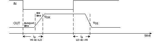
Propagation delay of a gate is not the same thing as rise or fall time for an individual transistor. To propagate through an IC a signal may have to pass through several transistors and may pass through different transistor paths depending on the kind of input (data, select, enable, etc) being asserted.
An npn bipolar transistor can turn on faster than it can turn off, which results in 7400
series chips having different propagation delays for LO-to-HI and HI-to-LO output
transitions. MOS transistors have a similar asymmetry-for a given channel width
n-channel MOS transistors are faster than p-channel MOS transistors.
S2#1--wire delay and RC time constant problem

S2 / 1 / 2 BOX: What causes propagation delay in logic circuits?
A small amount of delay in signal transmission is unavoidable because of the finite speed
of light, which travels one foot per nanosecond (signals move in wire at nearly the speed of
light). But most delay in switching circuits is due to the time it takes charges stored in one place
to move to another. The removal of stored charge from a capacitor through a resistance to
"ground" takes time, in the same way that emptying a bathtub through the drain takes time.
Electronic switches are made of transistors. Consider the input side of a common-emitter
transistor circuit, and the case of turning it off-charge caught in the base region must be
removed before the flow of current from collector to emitter is stopped. To a certain
approximation the base-emitter junction of a transistor acts like a capacitor.
When a bipolar transistor-inverter is ON sufficient base current can "saturate" the device
and fill its base region with electrons. The good news about saturation is that it lowers the
collector-to-emitter voltage-which represents logical LOW-to about
0.15v = VCEsat;
this lower output (VOL) means a good high level noise margin. The bad news is that a saturated
bipolar transistor takes time to turn OFF. It takes extra time to remove charge from the thin
base region. The region can be modeled by a parasitic junction capacitance, shown in the figure
below. The junction capacitance must be charged or discharged to or from 0.6v, in order to
complete switching. Remember Q=CV, where Q is charge, C is capacitance and V is voltage.
When base current stops flowing the transistor will still allow IC to pass (through the base, to the emitter, as electron "minority carriers" in npn) so long as "majority" charge is stored in the base. In one case, the excess stored charge in the base will be removed by "recombination of minority and majority carriers," a process which can take many nanoseconds. In another, the excess base charge may flow out through the resistor RB.
Saturation can be prevented by placing a Schottky diode from base to collector:
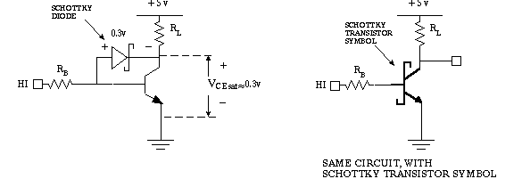
When the transistor is ON the Schottky diode diverts some of the RB current formally headed for the base, and "clamps" the base-to-collector voltage at about 0.3v, instead of the higher 0.5v. VCE is about 0.3v [and this slightly higher collector voltage reduces the DHL noise margin by 0.1v.]
S2#2--role of R sub L in switching speed of inverter
Another way to lower propagation delay-Decrease resistances around the chip-but if
RB is reduced too much then IB will reach a dangerously high level and might burn out the
transistor.
On the output side of a chip, capacitance associated with the load can
increase delay in transmission.
How is propagation delay decreased in CMOS? By reducing the "channel length." In
advanced CMOS, channel length can be fabricated at less than one micron.

S2 / 1 / 3 Delay in combinational gates
Propagation delay time is tP. For a combinational gate with one kind of input, like a
NAND gate on a 7400 chip, delay on data sheets is listed as tPLH and tPHL-the delay from
input to low-to-high or high-to-low OUTPUT switching. Sometimes data sheets list
only maximum values for each of these propagation delays, and in the case of the 7400
chip the values are
7400 tPLH for input to output 22 nsec, maximum
tPHL for input to output 15 nsec
Other variations for propagation delay in data sheets are minimum and typical. Usually a
designer is worried about the worst-case time, which, for a combinational chip, is the
maximum delay. Sometimes a minimum delay is cause for concern, to prevent race
conditions in flip flop circuits. Notice that the transistor turning off (tPLH) is associated with
the longer propagation delay; tPLH > tPHL .
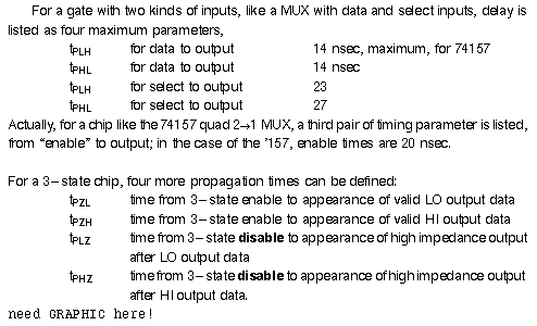
For other chips, with several kinds of input, there can be more timing parameters. The
24 pin Texas Instruments "multiport video dynamic RAM" chip 4461 lists in its data sheets
73 timing parameters, mostly as minimum values, but in some cases as minimum and
maximum. The 73 timing parameters are explained with the help of 18 timing diagrams!
You can see the varieties of timing in the DDZO chapter 8, Memory.
Propagation delay can have meaning for more than a single chip. It can be measured
or calculated for a hardware system with various data paths. The designer may have to
search for minimum and maximum delays. Maximum delay paths through digital systems
are called critical paths.
S2#3--interpreting data sheet AC parameters for MUX
S2 / 1 / 4 Flip flop timing
An un-clocked SR flip flop is graded by the propagation delay from SET or RESET to
changed output. SET or RESET must be on for a minimum duration of tW. Examples of flip
flop timing parameters are shown below for a clocked D flip flop with asynchronous SET.
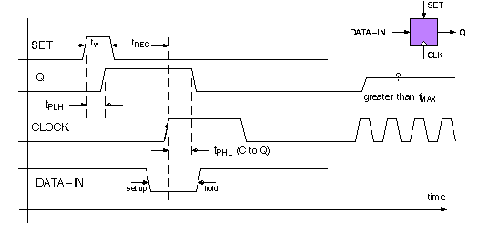
In edge-triggered flip flops we know from �5 that data input must meet set-up and hold times with respect to the clock edge, as shown above. In flip flops with both synchronous and asynchronous inputs, a parameter tREC, recovery time, can be defined which measures the amount of time after a SET or RESET that a CLOCK pulse will be recognized. A single parameter that somewhat summarizes the performance of a clocked flip flop is fMAX, the maximum clock rate in Hertz the chip can handle before errors occur.
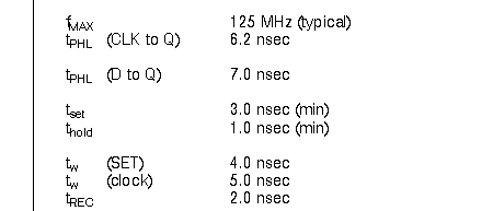
Example 1. Timing parameters for a 74F74 D flip flop are given below:

S2 / 2 Power consumption
Designers of electronic logic gates (IC's) fight with the tendency of switching circuits to
use more power the faster they switch. Why the concern about power consumption?
(1) Need for a larger power supply, and the cost of the power from the electric company. If
the unit is not plugged in, batteries will drain more quickly the more power consumed per
chip.
(2) Power consumed by a chip ends up as heat. Because heat degrades the performance
of an IC, and enough heat can burn it out, cooling systems must be installed where too
much heat will be generated.
S2 / 2 / 1 Box: Defining power
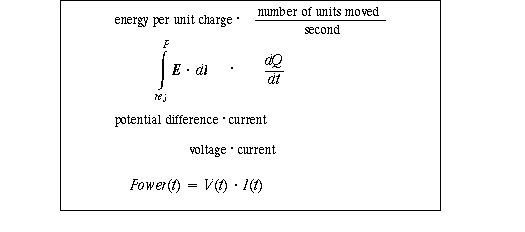
What is Power? Power = energy / sec.
Recall from mechanics that energy (or work) is force x distance.
Example 2. A 7 kg mass bowling ball slowly raised 0.5 meter against a gravitational force
gains 7 x 9.81 x � = 3.5 joules of energy.
Where 9.81 is the gravitational constant in MKS units.
In electricity, F = q�E, where E is the electric field vector. An electron with a charge of
-1.6x10⁻¹⁹ coulombs moved slowly � meter against an electric field of 1 volt/meter
gains 1.6x10⁻¹⁹ x � = 8x10-18 joules of energy.
Power is the rate of energy production or consumption. If U(t) is the energy of a system at time t,
then power is dU/dt, measured in joules/sec, or watts. Power can either be generated or
consumed by a system. The power company and a "power supply" are aptly named,
although a power supply normally transforms AC into DC, and is not a primary generator
of electrical power, as the rotating machinery of a power plant is.
As you may know, to compute power consumed in an electrical component, multiply
voltage across the component times current flowing through. The diagram below shows
the voltage and current conventions for positive power absorbed by a resistor:
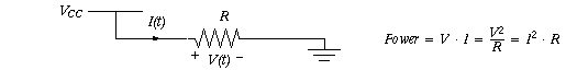
Below the formula for power in terms of current and voltage is developed.
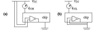
We include a time parameter in the power formula as a reminder that power can be an instantaneous quality. To compute steady-state or DC or average power consumed by a chip, multiply supply voltage VCC by supply current ICC. Supply current is listed in the data sheet for a chip under "DC" or static characteristics; it is usually listed two ways, ICCL, and ICCH. ICCL is the current which flows into the chip when all inputs are connected to LO; ICCH is for all inputs connected HI.
Example 3. The 7400 quad NAND gate the Signetics data sheet shows
7400 74LS00
ICCL = 8.0 mA 1.6 mA, maximum, and
ICCH = 12 mA 4.4 mA, maximum
where LS stands for "low-power Schottky."
Below are two circuits for showing ICCH (a) and ICCL (b).
static, dynamic power.
Data sheets for a chip list ICC, supply current for a chip with the understanding of no load
on the output pins. If VCC is 5 volts, then power, in watts, is
5 x ICC = Power consumed by the chip.
Connect the ammeter between the power supply and the chip to monitor ICC.
Example 4. How many 7400 chips would it take to [change a light bulb?] consume the same
power as a 100 watt light bulb? The data sheet for a 7400 chip lists
ICCH at 12mA = 12 x 10-3 amps,
so each chip consumes 5 x 12 x 10-3 = 0.06 watts. 100
0.06 � 1600 chips!
Actually, the voltage supplied to a light bulb is of the form V(t) = 170 cos (2p60�t) volts;
110 volts is the root-mean-square value of V(t). The time-varying voltage from the power
company is converted to steady ("DC") voltage in a power supply.
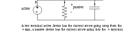
When a power supply delivers power to its output ports it is an active device or system; a passive
device, like a resistor, absorbs power. The figure below shows conventions for
Integrated circuit chips are power-absorbing devices. A passive device which absorbs
power gets warm. A light bulb absorbs power from the power company and radiates a
little light and a lot of heat.
Some chips, particularly display drivers like the 7448 , may get hot to the touch because
they're consuming a lot of power for their small size, sending current out to display
segments-an "8" signal should feel hotter than a "1."
Dynamic power dissipation-The charge stored on a capacitor is C�V, where V is the voltage
across the plates. Imagine moving the charge on a load capacitor CL as the output
changes from 0 to VCC. The average voltage the charges will see is �VCC, and the total
amount of charge moved will be CL�VCC. Since voltage is the energy required to move a
unit charge across the capacitor, the total energy stored in the capacitor is �
CL�(VCC)2. If the output switches at a rate* f per second, then the power, or energy per
second, dissipated by the switch is
f�CL�(VCC)2 called dynamic power dissipation.
[reference: Sedra & Smith, 3rd Edition, p. 914]
For TTL gates the dynamic power dissipation is not appreciable compared to the static
power dissipation until high frequency (MHz) rates of switching are seen. For CMOS
gates dynamic power dissipation is the main form of power dissipation; power consumed
by a CMOS chip is almost linear with frequency of switching.
Electrical power runs the world.
Delay-power product. Multiply [power x time] and units of energy result. Multiply the
delay (time per state switch) and power consumed by chip, and you have energy used per
state switch. For example, a 7400 chip has a maximum delay-power DP product of about 20 nanoseconds x 5v x 10 mA = 1000 pico Joules, while a 74LS00 has a maximum DP of 150 pJ.
Relationship between power & speed. If you inspect data sheets of chips from
different logic families, you'll find that switching speed increase is generally accompanied
by an increase in current delivered to the chip. For example,
chip ICCL tPHL DP product
7400 12 mA 15 ns 900 pJ
74S00 36 mA 5 ns 900 pJ
The 7400 uses less current but switches more slowly than the 74S00, but both chips have
the same DP product. Low-power Schottky chips have considerably lower DPs and so are
to be preferred over regular TTL and plain high speed Schottky chips.
Heat. The generation of heat would not be a matter of concern to us were it not for the
fact that semiconductor switches can be destroyed by high temperatures. Why does heat
damage chips? Semiconductor crystals are created at 1200�C, so who cares if power
consumption on a chip turns up the temperature a few hundred degrees? In commercial IC
devices, however, aluminum is used as a metallization layer for routing of wire-like
connections. Aluminum in contact with silicon melts at around 550�C; the melted metal can
cause a short circuit through a junction, or it can be plastically distorted to become an open
circuit. Since local temperature can be higher than the average temperature, aluminum
spiking can occur before the chip temperature reaches 500�C. There's not really much
disruption of the semiconductor crystal structure from excess heat in chips.
Electrostatic-not heat-damage to CMOS can cause a filament of metal to blast
through a junction, and thereby produce a local short circuit. Catastrophic failure from heat
is not the only concern. Higher temperatures can cause chips to operate at slower speeds.
Texas Instruments, "Manufacturing Process of Integrated Circuits: Sand to Circuit," a 40 min. VHS
color video tape (1991).
In some cases, such as processing radar or video in real time, the fastest chips
obtainable must be used, and the costs in power consumed, heat generated and circuits
artificially cooled must be paid.
Think of the heat generated by the muscles of the animals below.
from The Far Side Gallery 3, by Gary Larson
S2 / 3 Families and super-families
In a narrow sense a logic family is a set of small and medium-scale integrated circuits,
fabricated from a common process, which span the range of gates and flip flops that a logic
designer may find useful in assembling a large digital system. Like Classic Coke mutating
into New Coke, Diet Coke, Cherry Coke and Caffeine-free Coke, successful logic families
evolve new sub-groups and become super-families. Only two digital logic technologies
are in the super-family category: transistor-transistor logic (TTL) and complementary
metal-oxide-semiconductor (CMOS). TTL was not the first logic family, but by the late
60's chips in the 7400 series had a combination of shorter propagation delay and lower
power consumption, compared to the now obsolete families of diode logic,
resistor-transistor logic, and diode-transistor logic. TTL chips in dual in-line packages
(DIPs) filled the circuit boards of computers.
CMOS started out in the 1970's as the 4000 series family, but its virtue of low static
power consumption, and breakthroughs in speed thanks to narrow channel fabrication,
have allowed CMOS to become the technology of choice for highly integrated circuits. In
1991 CMOS is the most widely used digital logic process. The CMOS process is applied
widely to memories, microprocessors and gate arrays-the kinds of "LSI" chips not
generally considered in a particular logic family.
S2 / 3 / 1 The TTL super-family
In 1965 TTL was the first process technology able to be fashioned into integrated
circuits which had a good combination of high speed and low power consumption. TTL is a
bipolar process in which npn transistors operate mostly in the "saturated" and "cutoff"
regions of their operating curves. Below we list delay and power dissipation specs of
various TTL families.
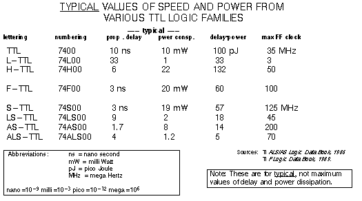
7400, 74L00, and 74H00 chips are "gold-doped" in the fabrication process; all chips with "S" is the letter designation have Schottky diodes from base to emitter on transistors which can saturate. In the lettering scheme, "L" stands for low-power, "H" stands for high speed, "F" stands for fast, and "A" stands for "advanced."
[Propagation delay the average of tPHL and tPLH; power consumption = 5 x �(ICCH + ICCL)]
All 74 TTL families are shadowed by 5400 families which meet military specifications for
wider tolerance to temperature variation.
Sample costs in 1991: 74LS00 31�, 7400 36�, 54LS00 69�; [74L and 74H series, obsolete.]
In 1965 a 7400 chip cost around $20!
S2 / 3 / 2 The CMOS super-family
Once just another member of the MOS group, CMOS has become a super-family of
its own. In the 1970's the original appeal of CMOS, compared to TTL, was its low power
consumption and wide tolerance for power supply voltages. CMOS chips filled a niche in
battery-operated devices, where voltage would slowly decline over the life of the battery.
The first CMOS family, the 4000-series chips, averaged just nanowatts quiescent power
per gate and tolerated voltages as low as 3 and as high as 18 volts for VCC.
- CMOS families: speed, power, noise, fanout...
4000, 14000 (Motorola)
B - series
74C00 same pinout as 7400 TTL series
74HC00 H for "high speed"
74HCT00 for interface to TTL chips
74AC00 "advanced"
74ACT for interface to TTL chips
see Advanced CMOS Logic, Designer's Handbook, TI, 1988.
and High Speed CMOS Data Book, TI, 1989.
CMOS Logic Data , Motorola, 1990.
See Wakerly, page 129 for 1989 CMOS data table.
CMOS logic and propagation delay. MOS stands for
"Metal-Oxide-Semiconductor," and is a description of the top-to-bottom layers in a
MOS chip. The oxide is silicon dioxide, a hard insulating material. The metal is in the form of
thin interconnecting strips from one gate to another.
PHOTO OF IC?
The "C" in CMOS stands for complementary, in regard to the "doping" of the two
transistors which make up the "totem pole" output.
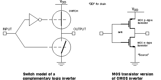
Again we see our splitter diagram on the left, mimicked on the right by two MOS transistors, one p-channel, the other n-channel (complementary to each other). These MOS transistors act as switches-only one can be closed at a time. Thus CMOS chips consume almost no power when they are not switching. When a CMOS inverter switches, there is a brief time when charge can flow through both transistors. Power consumption in CMOS devices is proportional to switching frequency.
CMOS is a NAND-based family, like TTL. A CMOS 2-input NAND gate is shown
below in (a). A switching circuit interpretation is in (b). Notice there are 2 kinds of switches,
one SPST which closes in response to HI, and another which opens. Also, no resistors are
needed in the CMOS circuit, other than the resistances of the gates themselves.
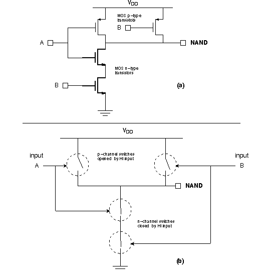
Otherwise the switching circuit above looks like the EXOR gate designed in �1. Both inputs are HI in the case above, causing OUT to be grounded.
Power supply tolerance (=range of acceptable power supply voltage) is much greater
in CMOS than TTL. Because of low power consumption and tolerance of power supply
voltage, CMOS is favored in consumer electronics powered with batteries, such as digital
watches (where, also, low-power liquid crystal displays are favored over LED's). More
modern CMOS families, such as ACT or HCT, are designed to operate around a narrower
power supply range, such as 2-6 volts.
S2 / 3 / 3 Bipolar - CMOS hybrid
TTL-CMOS interfacing between logic levels was discussed in the previous �. Here we
draw your attention to a logic family BiCMOS, which uses CMOS transistors for input, and
bipolar (TTL) transistors for output. The result is a hybrid logic family with good packing
density, low power consumption, and excellent speed. The CMOS front end results in high
input impedance and good noise margin, and high fanout. BiCMOS chips provide an
automatic interface from TTL to CMOS, and are comparable to TTL-AS in speed and
better with regard to power. A 74BC00 chip consumes 6mA of current when output is LO,
and 10 mA when output is HI. It's propagation delay into a 50pF-500W load is 3.8 nsec. A
BiCMOS flip flop can operate at up 100 MHz clock rate.
Motorola BiCMOS Logic Data (1990).
S2 / 4 Logic families specialized for speed
TTL chips are generally faster than CMOS gates (but see ACT series), however there are
two logic technologies faster than TTL-Emitter-coupled logic (ECL) and gallium
arsenide (GaAs). These chips come at considerable cost in power consumption and ease
of interface to other logic families. Chips in the TTL AS family, and CMOS HC family are
quite fast, consequently the motivation to use ECL parts has dropped in recent years.
S2 / 4 / 1 Emitter-coupled logic (ECL)
ECL technology has been around longer, so let's consider it first. ECL is a
non-saturating type of silicon bipolar design. TTL is a saturating bipolar design. Keeping
transistors out of saturation decreases propagation delay (and minimizes amount of
switching noise generated). The boxed material can start you understanding how a basic
ECL inverter works as a "differential amplifier." Instead of switching voltage levels at one
output, ECL switches current flow in two arms of the circuit; one byproduct of ECL
switching: Both a variable and its complement are available as chip outputs. Within its
family, 10K ECL has good fanout. Interface to TTL and CMOS is awkward because of
different power supply ranges.
Noise margins, measured in volts, are much smaller in ECL than TTL, but there is some
compensation in the fact that ECL circuits are less noisy than TTL. Propagation times for
commercial ECL families are close to one nanosecond. Unfortunately ECL chips consume
a lot of current, up to 60mA per gate in the 100K family.
ECL gates can be thought of as current mode devices, where current flows through one or
another arm of the differential pair, depending on the state of the circuit.The basic ECL
inverter design, shown below, starts with a transistor over an emitter resistor, like we've seen in
the TTL splitter. The idea will remind you of an analog differential amplifier.
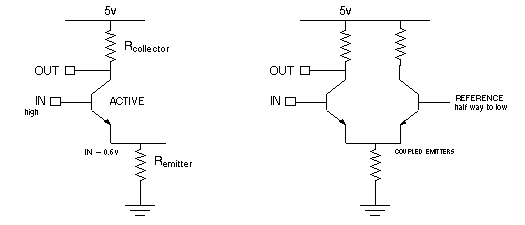
On the right above is shown the emitter-coupling which is the basic building block of ECL; current through either transistor will create a voltage drop across Rem. Let a high IN = 4.4v. If the ratio of Remitter to Rcollector is carefully adjusted, then Remitter limits the total current through the transistor and keeps the transistor out of saturation. Depending on the state of the ECL switch more current will flow through one or the other of the collector resistors. Unconnected ECL inputs float low.
In commercial ECL families (10K is the most popular) the power supply is actually -5.2
volts, connected where ground is above; +5 in the drawing above is at ground. With the power
supply on the common emitter resister Rem, the circuit has more immunity to spikes on the
power lines, and in fact ECL has much less problem than TTL with switching spikes, since ECL
current magnitudes do not change during transitions.
Great care must be taken with the construction of ECL circuits operating near their
maximum clock rates; for example, ordinary wires connecting chip outputs and inputs must be
less than 10 cm, or be made as terminated transmission lines, to avoid spurious ringing.
Motorola MECL Device Data (1989) &
Motorola MECL System Design Handbook (1983).
These books describe the 10K logic family.
S2 / 4 / 2 Gallium Arsenide
Gallium Arsenide (GaAs) chips are not based on silicon. Silicon, like carbon, is in
column IV of the periodic table. Gallium is in column III and arsenic in V. Depending on the
ratio of Ga to As, a mixture of gallium and arsenide can have a crystal structure with a
desired conductivity. GaAs is a semiconductor with higher mobility.* GaAs chips can
switch as rapidly as ECL, in the sub-nanosecond range, but consume only � the power.
GaAs materials, however, lack a hard insulating oxide comparable to silicon dioxide, so
GaAs semiconductors are limited in the gate packing density which can be achieved. *
It would seem that purveyors of a new technology, such as GaAs, would consider
implementation in general-purpose "gate arrays" to finesse the problem of
manufacturing the hundreds of standard chips needed to compete with established
families of TTL and CMOS. GaAs is less evolved as a logic family than ECL, in fact there is
no standard GaAs family. See offerings by Gazelle Inc. and Vitesse Corp. Gazelle produces
a 22V10 PAL with 5.5 ns tpd. Besides digital, GaAs transistors have numerous applications
in high speed analog design.
(3) Mun, Joseph, (ed) GaAs Integrated Circuits-Design & Technology, Macmillan Publishing, 1988 TK7874 / G33 See chapter 3, "Digital integrated circuit technologies."
S2 / 5 Packing density
All other things being equal, shorter connections will make for a faster circuit. And
shorter connections will have less loading capacitance. The shortest connections are
made directly on the integrated circuit chip itself. Such IC connections must be made by
photolithography; they are more reliable than hand or machine connected wrapped wires
or printed circuit board routing. As a result, the number of gates per IC, the packing density,
can be an important factor in selecting a logic family for a job. In the regard of packing
density, CMOS is the leading technology. CMOS memory chips with 64 million transistors
have been fabricated.
S2 / 6 Chart comparing logic families
The following chart compares, qualitatively, state of the art TTL and CMOS with ECL
100K and GaAs logic, in 7 different categories.
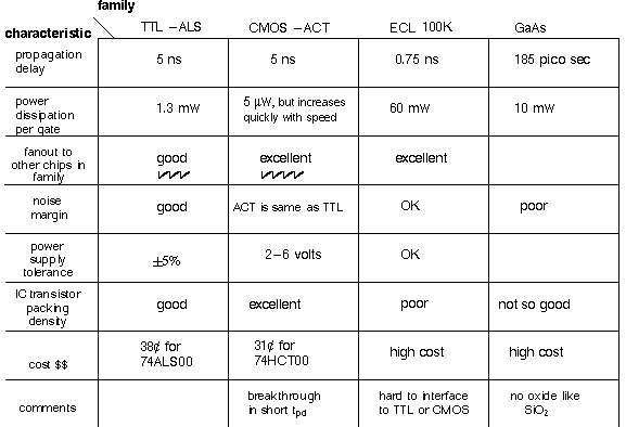
Not so fast.
Input: A matter of noise margin. In a densely packed integrated circuit, with thin
interconnection wires (1-3 mm), some gates may see power supply voltages and signals
which have been contaminated by noise. How well the gates reject the noise can be an
important consideration, but not as important as speed, power consumption and packing
density in the scale of things. Fortunately, as we know, digital circuits can be quite forgiving
with regard to variations in LOW and HIGH signal ranges. This, in fact, is one reason digital
IC's have progressed to much denser packing than analog IC's. Switching speed, our
primary digital IC quality, is perversely related to noise produced in chips and systems. The
faster the transition from one state to the other by a switch, the more current transients
generated by the switch and throw noise (either as local E-M radiation, or a power supply
glitches) into the neighboring system. In the special category of memory IC's, problems
can arise with regard to the altering of memory contents by EM radiation, and from
radioactive decay in the packaging material (thorium contamination of ceramics).
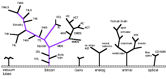
Evolutionary "forest" of digital logic and other intelligence:
S2 / 7 Logic families vs programmable logic devices
The invention of the microprocessor in the 1970's started an era in which
general-purpose large-scale integrated circuits could be called upon to perform many
logic tasks (central processing in a computer, for example) formerly done by circuit board
assemblies of chips from particular logic families. Small- and medium-scale integrated
circuits in the form of gates and flip flops from logic families then become "glue" in the
service of the large chips, providing specialized interface capabilities. In the 1990's
"random logic" (SSI and MSI gates from logic families) will be more and more replaced
with programmable logic devices (PLDs) such as field programmable gate arrays
(FPGAs). A designer will no longer leaf through a data book looking for a chip which does
some of what he or she wants; rather the designer will layout and simulate with software his
or her ideas for a design, then program a general-purpose chip to implement those those
needs. In both cases, whether with gates and flip flops from a logic family or with a FPGA,
chips are the final product, but with FPGAs it may be only one chip, and that chip may have
as many as 176 pins.
The question to answer: What logic families do FPGAs and other PLD's belong to? The
short answer is CMOS. CMOS is the preferred technology because of the ease with which
many transistors can be placed on one IC, and because of the low power consumption of
the resulting configuration. Modern CMOS fabrication results in speeds which approach
advanced TTL. Except in cases where the fastest speed is an essential requirement of a
design, CMOS gate arrays will be the dominant technology for random logic hardware in
the next decade.
Especially through the 1970's the 7400 series of TTL gates, at small and medium scale
integration were used for much of digital logic design, especially the CPU's of high speed
computers. However, starting with memory chips, and later progressing into monolithic
microprocessors, MOS fabrication took increasing market share. Especially in low power
CMOS form the greater packing density of MOS technology assured it an improving
"survival" rate. In some cases it's possible to combine both technologies in a single chip:
BiMOS as it's called. Now-a-days most IC's can be accommodated with MOS
technology, except in high-speed requirements, where bipolar ECL, and now GaAs,
remain necessary. Supercomputers maintain their high speed by short interconnects as
well as by fast chips. Random logic, picked by an engineer to optimize a particular design,
is now being replaced by standard gate arrays, which have more in common with
systematic memory organizations than with Karnaugh-map & excitation map minimized
designs.
New Technology. Carbon is in the same column of the periodic table as silicon.
Integrated circuits are not based on carbon because carbon is not easily turned into
crystalline form. Carbon in crystalline form is called diamond. Recent progress in
synthesizing diamond may make carbon a realistic atom on which to base future forms of
integrated circuit (Science 252: page 375, April 19, 1991). Diamond IC's would be faster
and have better heat characteristics.
And see Nature 350: 561-62, April 18, 1991, "Dawn of the diamond chip," by L.M.
Brown. Review of work from Japan on the development of diamond p-n junction diode.
Diamond has better thermal conductivity than silicon; diamond chips might be able to
operate at 1000�C. Perhaps the elusive blue LED could be constructed on diamond
substrate.
October 1992 Scientific American page 84, "Diamond Film
Semiconductors," by M. W. Geis & J.C. Angus. Best thermal conductivity
of any material at room temperature. Diamond semiconductors would
operate at high speed, high temperature. Diamond is a metastable state
of carbon.
S2 / 8 Summary
- Propagation delay is the time between presentation of input and change of output to a
new logic level. For modern solid state logic gates propagation delays are in the range of
nanoseconds.
- If it has different kinds of inputs, such as data, select, enable, etc, one logic chip will need
several propagation delays to specify it, depending on which kind of input is tested
versus output.
- IC chips consume power in either static or dynamic modes. Dynamic power dissipation
is proportional to rate of switching and is important in CMOS chips.
- IC Power consumption is generally correlated with propagation delay-all other things
being equal, the shorter the propagation delay, the more energy used by the switch.
- A delay-power factor allows for comparison between logic gates; the lower the DP
factor, the better the gate's performance.
- Power consumption results in heat production, which can degrade chip performance
and, if it exceeds limits, can irreversibly damage the chip. Excess heat may precipitate
another cost-cooling of a circuit. In the future, solid state circuits based on synthetic
diamond may prove more heat resistant than any current logic family.
- High speed switching can result in generation of large current transients, which sneak
around the power supply wires, invading other chips, like gremlins.
- Transistor-transistor logic (TTL) is a bipolar super-family with many sub-families,
coded 74FamXXX. The most important TTL subfamilies are the ones which incorporate
Schottky diodes to increase speed without excess increase in power consumed.
- The Complementary Metal-Oxide-Semiconductor (CMOS) super-family has
several sub-families compatible with 7400 series pinouts. Compared to TTL, CMOS
chips dissipate less power, are more tolerant of power supply voltage variations, and can
pack more transistors per chip. CMOS technology is applied to microprocessors,
memory and FPGAs.
- Emitter coupled logic and Gallium Arsenide technology are two of the fastest forms of
electronic logic; GaAs gates in particular have sub-nanosecond propagation delays.
ECL and GaAs gates consume much more power than TTL or CMOS gates, and can't be
fabricated to the high level of integration that TTL or CMOS can.
- A comparison of logic families suggests that a designer must make choices on the basis
of power dissipation, propagation delay, $$ cost, packing density, fanout, and noise
margin.
(4) Wakerly, J., Digital Design, Principles and Practices, Prentice-Hall (1990) See chapter
2, "Digital Circuits"
(5) Ferry, Akers & Greenwich, Ultra Large Scale Integrated Microelectronics, Prentice-Hall (1988) TK7874 / F46
*The rate in this discussion is not the number of transistor switches per second;
internal switches/sec is twice the rate of the output switching.
After Carver Mead, Analog VLSI and Neural Systems, Addison-Wesley, (1989) * Imagine a charged particle q in a wire, subject to an external electric field E.
F = m�a = q�E
where m is the mass of the particle, and a is the particle's acceleration. The particle collides with other
particles in the wire. It travels a distance s in time tf between collisions. The relationship between s
and tf is The average drift velocity of many colliding particles subject to the force is where m is mobility. In GaAs tf is less than in silicon, therefore its mobility is greater.
*See Scientific American, February 1990, for article on Gallium Arsenide by M.H. Brodsky.
Another reference-Michael Shur, GaAs Devices and Circuits, Plenum Press, New York, 1987.
1/90 From a review in Nature, 26 May 1988, by John Barker. "Silicon has achieved its present
supremacy by a scaleable technology which can accurately produce digital logic and memories
which are not only fast but which have high-integration densities. The key [for silicon] is the
existence of a well-matched insulator, silicon dioxide, which provides the basis for the highly
controllable metal-oxide-semiconductor field effect transistor technology."