S5 A Microprogrammed CPU
And what rough beast, its hour come round at last,
Slouches toward Bethlehem to be born? W.B. Yeats
Link to End of Chapter Exercises
S5 / 1 The Second Coming
In the last chapter of the DDZO text we glimpsed, through the binoculars of register
transfer logic, a sphinx of a computer. In this final supplement we approach more closely to
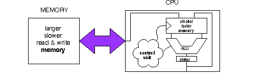
the computer, and try to solve its riddle. A computer can be divided into a central
processing unit (CPU) and a read/write memory system. The CPU can be partitioned
further into a combinational arithmetic-logic-shifter unit surrounded by clocked registers
and controlled by (what else?) a control unit.
The major riddle in a computer is the control unit, and that will be our focus in this chpt. We
will study a systematic approach called microprogrammed control. Before we explain
microprogramming, we outline a CPU architecture to be controlled, with inspiration taken
from the AMD 2901 single-chip registered ALU "slice." And before we slice open the (now
obsolete) 2901, we step back to consider the place of the human in all this--
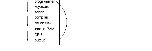
The information flow above addresses two questions often asked about a computer: "How does its memory fill up with information?" and "How does data get into its registers?" It can all starts with a human typing at a keyboard.
S5 / 2 2901 jr.
Here are an ALU & registers, in the architecture we'll design a controller for. Like some
of the multi-register machines we saw in Chapter 11, this one has a MUX insinuated
between the registers and the two ALU inputs.
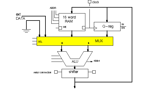
Two other choices appear on the MUX inputs--all zero's and EXTERNAL DATA. EXTERNAL DATA can be an entry point for data from memory. The MUX has two outputs, labelled R and S, which then project to the two ALU input ports. The number of combinations of 4 things taken two at a time is
so 3 bits of MUX select are needed to select all input combinations. Such a calculation assumes that the two input ports to the ALU are treated equivalently by the ALU operations, which may not be true (think about subtraction).
Via the 4-bit address, the 16-word RAM allows one of its words access to the
SOURCE MUX. If write-enable is active, then the output of the shifter will be written to the
RAM location specified by the address, when the clock is LO. Like the SRAM's we
considered in chapter 8 DDZO, the write-enable is level-, not edge-sensitive, in the 2901
RAM.
Since writing is a level-sensitive operation, the RAM system needs an output latch (slave,
not shown above) to avoid data racing around from shifter to RAM and back again.

If the latch is transparent when clock is HI, and holds previous data when clock is LO, then racing will be prevented.
The output of the shifter will be written to the Q-register on the rising edge of a clock pulse if the register is enabled, otherwise previous data is held.
The ALU is an eight-function combinational circuit with CIN with several status
outputs. Three "instruction" pins select one of the functions. The functions are--
R plus S
S minus R
R minus S
When CIN = 1 the subtraction is 2's complement.
R OR S
R AND S
R AND S that's R-bar...
R EXOR S
R EXNOR S
The status outputs are
C-OUT
G
P
overflow
sign bit (MSB)
OUT = 0000
COUT is generated by internal carry-look-ahead circuitry and G and P are the CLA
"generate" and "propagate" signals for connection to a second-order CLA chip, the 2902.
Overflow = CN+1 � CN.
The shifter here has the same three choices (left, right, no-shift) as the shifter designed in
the previous �; the least and most significant bits are led out as pins for connection to
another "slice", or to define circular, straight, arithmetic, etc shifts.
S5 / 2 / 1 A real 2901
is a 40 pin bipolar TTL chip with a 4-bit data pathway. It has 3-state outputs from its
ALU. The output of the device comes from the ALU, not the shifter. The shifter is really two
shifters, one each for the Q register and for RAM. The RAM is "dual port" with two sets of
4-bit addresses (A & B) and two output ports to the Source-Select MUX. Only the RAM
location addressed by the B pins can be written to, but both addresses can be read from.
There are latches on each of the RAM ports, as needed to avoid race. The input MUX has 5
choices (zero, external, A-RAM, B-RAM, Q) and a subset of 8 of the possible 10
combinations can be selected (B-Q & B-D are not possible).
One 2901 is intended as a "slice" of a larger 4xN bit CPU; since RAM and Q have their own
shifters, 4 pins (RAM0, RAM3, Q0, and Q3) must be connected with neighboring slices.
To complete the slice connections, hook the CN+4 pins of lower order slices to the CN pins
of their neighboring higher order slices.
Because it has a clock, the 2901 speed should be gauged by its maximum clock rate, which
for the 2901C is 15 MHz. Propagation delay from clock to output pin "F3" is 50 nsec.
More information about the 2901 can be obtained from the AMD data book cited below, or
JD Lab Manual +. AMD subsequently developed the 48-pin 2903 4-bit "super slice," with
16 ALU instructions. See an old AMD data book for comparison.
The 2900 series of chips is fabricated with bipolar, not MOS, technology. At the time it
was designed, the 2901 was much faster than any CMOS microprocessor or memory
components. In particular, its 16 word "cache memory" had much shorter access times
than the dynamic RAM used in main memory.
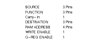
There are nine other pins on the 2901 we haven't mentioned yet--instruction pins.
Three pins each to instruct the 2901 about which SOURCEs for ALU input, which
FUNCTION for the ALU to perform, and what DESTINATION the ALU output should go to.
Since the shifters on the real 2901 are closer to the destination RAM and Q registers, shifter
function is specified by the DESTINATION "field" of the instruction.
We already know what eight arithmetic and logic operations the 3 FUNCTION pins can
select, and we know that the SOURCE field select a pair of inputs from among a choice of 4
or 5 MUX inputs.
The eight destination instructions, in RTL notation, include
RAM z ALU (write the the ALU output to RAM)
Q z ALU (load Q)
no-op (nothing loaded; just let a clock cycle pass; used as a wait state)
RAM z RAM/2 ; Q z Q/2 (shift RAM & Q down)
RAM z 2�RAM ; Q z 2�Q (shift RAM & Q up)
where "RAM" means the RAM location addressed by the "B" pins.
Advanced Micro Devices Bipolar Logic and Interface Data Book. AMD, 901 Thompson Place,
Sunnyvale, CA 94088.
G.J. Myers, Digital System Design with LSI Bit-Slice Logic. John Wiley & Sons, New York,
1980. See chapter 3, "ALU/Register slices."
Mick & Brick, Bit Slice Microprocessor Design, McGraw-Hill, New York, 1980. See
chapter III, "The data path."
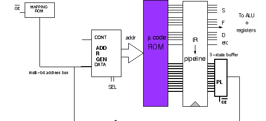
S5 / 2 / 2 Instruction and status registers
Now that we have a registered ALU in hand, we can design a controller for it. Before
doing so, we list the pins which will attach to the controller.
That's at least 16 pins, much more than 4-bit data path of one of our registered ALUs.
That's OK. We'll call for a 16-bit register, and later need to add more bits as the instruction
register evolves to a "pipeline" register.
The registered ALU will return six status signals to our controller, which can be used for
conditional branching in the microcode.
The machine's status can be saved in another register:
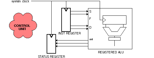
The instruction and status registers are an "interface" between the control unit and the registered ALU, as we have partitioned it, but all three share the same clock.

S5 / 3 Microprogramming
An instruction-a micro-instruction, more precisely-for one CPU clock cycle will
control all the SOURCE, FUNCTION, DESTINATION, ADDRESS, CIN, etc in the ALU and its
registers. All of the different micro-instructions that the CPU will need are stored in a ROM
whose many output pins*

project synchronously to the instruction register.

Thanks to a new clock pulse, the instruction register is loaded with the output of ROM. This
ROM is in the CPU; it is not in the memory system of the computer. The ROM is a
combinational circuit; the instruction register and address generator on either side of it are
clocked, but the ROM is not. To work effectively with the hardware in the ALU and registers,
the m-code ROM should be fast-brief propagation delay from new address to new data.
The many words in ROM can be divided into sections which represent higher-level
instructions, ADD or MULTIPLY or MOVE data to a different location, for example. In
general, a user instruction (higher-level instruction) has a FETCH and an EXECUTE
phase. The micro-instructions for FETCH may be common to many instructions, and so
may reside in ROM where they can be called as a subroutine. The 1's and 0's which make
up one micro-instruction can also be called micro-code. The art of micro-programming
(a level of programming below assembly language) is the art of writing micro-code, code
which defines the instruction set of a computer. We do not refer to m-code RAM; ROM
gives the correct impression that the m-code cannot easily be changed, and that should
be true about a computer's instruction set. These various facts about m-code ROM should
be kept in mind as we work through the main design problem of the micro-program
controller-the address generator.
S5 / 3 / 1 Address generator
If micro-code is written systematically, then next instruction from ROM will be one
address greater than the current instruction (an increment operation in the generator). But
there must still be some times when a JUMP to a dis-continuous location is required, for
example, every time a new user instruction is fetched.
We begin the design of the next address generator with a MUX which can choose between
an increment of the present address, Y+1, or a jump to a dis-continuous address, D:

There are two designs to consider for the CONTinue choice, an up-counter or a combinational incrementer + register:
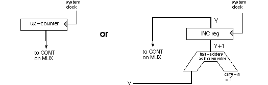
The up-counter looks simpler until we think about JUMPing. The incrementer + register handles jumping with no problem because the jump location D is automatically sent to the input of the incrementer. The up-counter, on the other hand, must have a LOAD feature, and it must be loaded with D at the same time D is passed out of the MUX. The load control for the counter must come from SEL for the MUX. Another feature in favor of the incrementer+register is that it maintains both Y and Y+1 internally, a state useful for saving a return address in a subroutine operation.
[An end-of-� exercise allows you to explore the propagation delay differences between the two designs.]
S5 / 3 / 2 The jump location
One source of jump location is the next instruction in the user's program stored in
system RAM (more precisely, the compiled version of the user's program, stored in an
assembly language "object file"). Another source can be the microcode, which is
executing, over several clock cycles, the user's current instruction. Since both of these
sources are outside the address generator itself, let's attach them to the D-input of the
MUX by a 3-state bus:
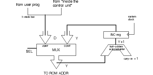
What exactly do we mean, that a jump location is in microcode itself? That the present set of bits in the instruction register has another field-the next address field-which projects not to the registered ALU but back to the address generator D input.
The next figure shows that the instruction register has been widened to accommodate this "next address" part of the microcode word. The next address passes through a 3-state buffer, then attaches to the address bus on the D-input of the address generator MUX.
Also attached to the address bus is the output of "mapping ROM," from the user program's next instruction. The mapping ROM "maps" an assembly language input to a m-code ROM address. The mapping ROM has a 3-state output. Later we will add output-enable controls to the address generator circuit, which will choose which, if either, of the mapping ROM or pipeline buffer should have control of the address bus.
"Instruction register" is no longer an appropriate name for the register which hold the ALU & registers & next address information. We rename it pipeline register. It's one register in a pipeline of information transfer from user program to CPU. A pipeline is a generalized shift register in which many bits are shifted in parallel.
How many bits might be in the address bus? Twelve bits would address 4096 m-code ROM addresses, and 12 bits is the width of the address bus in the 2910 microprogram sequencer. With 4000 locations and an instruction set with 50 entries, each instruction could take up an average of 8 microcode words.
The feedback pathway from the pipeline register back to the address generator is clear evidence that we are constructing a clocked sequencer (Moore circuit), like we did in �6. Here we are not vexed by the problem of minimizing the number of gates in the design. Before the commercial advent of microprogramming in the late 1960's CPU control circuits were "hard-wired" with tightly designed clocked sequencers. Now with the expense of a ROM and the delay of the pipeline, the process of designing the hardware for the controller can be separated from the task of designing the instruction set for the computer. To change the instruction set of a micro-programmed computer, simply change the code in the ROM.
For a good development of the "random logic" approach to control unit design see
Thomas Bartee, Digital Computer Fundamentals, 6th Edition, McGraw-Hill (1985) chapter
9, "The control unit."
Pause for a moment to appreciate the micro-program sequencer's "philosophy"; it
not only knows what it's doing now, but knows what it's going to do next. Look before you
leap, or in this case, look before you jump.
In fact the feedback has another component we haven't shown on the figure above:
The current microcode instruction also contains the SEL for the next-address MUX, so
that the current instruction can tell the address generator when to look at the D input.
The feedback arrangement providing for the next sequencer instruction makes the job of
writing microcode more difficult: Each line of mcode controls the current Source Function
Destination, etc of the registered ALU, and it must contain the next sequencer instruction,
and possibly the next sequencer D-address.
[There are some subtle timing issues with regard to the arrival of the next active edge of the system clock
and when the control unit finally settles to the next instruction in the pipeline-propagation delay-but we
defer these issues until later in the �, and to the Lab Manual. ]
S5 / 3 / 3 One-level subroutine
So far our next address generator, or sequencer, has no more capability than an
up-counter with LOAD. Now we take advantage of the incrementer-register to save the
next continue address address during a JUMP, then return to that address after executing a
"subroutine". See address blocks below.
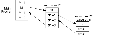
Here "Main Program" means the code address sequence in micro-code ROM.
The sequence ... M-1, M, S, ... S+3, M+1 ... must be stepped through.
Two sequencer instructions will be needed for the complete process: JSR, for "jump to
subroutine" and RTS, for "return from subroutine." Again, to motivate*
interest in
subroutines we remind you that the microcode may be structured to include a common
FETCH subroutine in each micro-coded instruction. FETCH can obtain the next user
instruction from main memory, and increment a "program counter" register in the ALU
register set. We don't have to be concerned about what happens in the subroutine, just
about going to the subroutine and getting back to M+1 in the main program when the
subroutine is finished. Since FETCH is used by many instruction code sequences (such as
program N, above), it cannot have built in a unique return address. In one case return is to
M+1, in another to N+1.
Saving the current address + 1. When a JSR instruction arrives at the microprogram
sequencer, the address M+1 must be saved in another register. Call that register R and
give its output a third access the address generator MUX, as shown below. R-reg has
been placed above the INC-reg, extending the internal pipeline of the microprogram
sequencer. The timing problems associated with placing R-reg at the same level as
INC-reg can be explored in an end-of-chapter exercise.
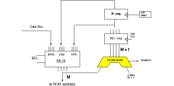
When the "pop" input on the MUX is selected the current output of the R-register becomes the ROM address. The circuit above has its own timing problem, which is easier to solve-If a new clock edge sends M+1 to the INC register before the "JSR detect" signal arrives at the R-reg, then the correct M+1 value will be written into the R-reg.
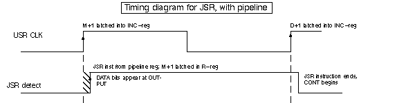
Insure that the R-reg clock occurs tset-up after user clock, and M+1 races through the INC-reg to land where it should in R-reg.
When the subroutine is finished the return location is available at the output of the
R-register, and a MUX select to POP will bring address M+1 to the output of the address
generator, as desired.
S5 / 3 / 4 Nested subroutines
By turning the R-reg into a last-in, first-out "LIFO stack" the sequencer can handle
nested subroutines.
Subroutines can be nested to a level as deep as the stack; let's say 4-deep for the example we're working. The LIFO stack can be a 4-word memory addressed by 2 bits from an up/down counter known as the stack pointer.
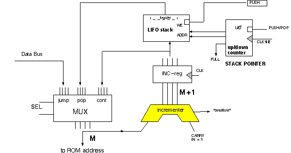
There are two control signals for the stack- SE = stack-enable, which is active for both JSR and RTS instructions, and PUSH/POP, which is HI (PUSH, count up) for JSR and LO (POP, count-down) for RTS. SE is AND'd with the system clock to produce clock edges for the stack pointer. If more than 4 JSR's are attempted before an RTS, then the "FULL" warning is lit by the stack pointer.
For one-level subroutining only the clock on the R-reg need be coordinated with the clock on the INC-reg. Now the clock on the counter, the up/down control, and the stack write-enable need to be coordinated with INC-reg. In particular, note that SE may increment or decrement the counter near the system clock edge, but for an RTS the counter may present an incorrect value to the POP input of the MUX. This problem can be overcome by sticking another "pipeline" register at the output of the stack, and changing the phase on which the stack point is changed. See details in an end-of-� problem, or JD Lab Manual.
S5 / 3 / 5 Conditional branching in microcode
We advertised that our sequencer would be able to handle conditional branching.
Conditions to cause branching can come from three sources:
� *The user program
� *Internal conditions collected by the status register from the ALU.
� *External conditions, like EOC from an A/D converter.
Changes in microcode address from the user program are expected and are handled by
the "mapping ROM" shown earlier, which has 3-state access to the sequencer data bus.
Feedback from the status register. "Internal" conditions will come from the status
register which saves COUT, overflow, sign bit, zero-detect, etc from the ALU operations.
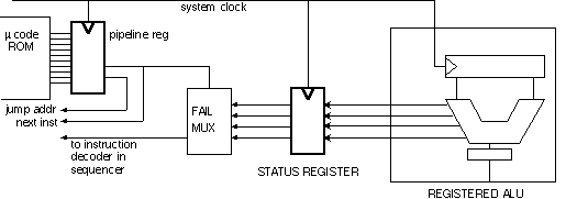
Shown above is a "FAIL MUX" which uses the next sequencer instruction, stored in the pipeline register, to select an appropriate status bit to check. For example, if the user instruction is a signed addition, it will be important to check for overflow, but not for carry-out. We show the output of the FAIL MUX headed to a sequencer instruction decoder, which will be explained in a couple paragraphs.
External interrupts. Events in this category may be unexpected, or occur at
unpredictable, even asynchronous times, but their possible occurrence has been planned
for in the form of interrupt service routines in microcode. In this � we ignore external events
whose occurrence does require urgent attention and who can be handled by scheduled
"polling" of the flags and status bits in external devices.*

Here we outline how a CPU
controller can manage "real time" events-some welcome, like a signal that a
co-processor has completed a floating point calculation, some unwelcome, like a power
failure during which time the controller may have 100 msec to start and finish a shutdown
procedure. Interrupt service sub-routine addresses can be announced to the controller
the same way user instructions are, through a 3-state output ROM, in this case called a
"vector ROM," to suggest that the ROM supplies a vector pointing to the proper interrupt
service routine:
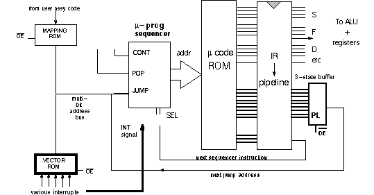
The interrupt signals, which may have to pass through enabling, synchronizing, and pulse-capturing circuits, form the address to the vector ROM. The output of the vector ROM is an address in micro-code ROM where the interrupt service routine starts.
[Additionally, a signal that an unexpected interrupt has occurred may be sent directly to the sequencer.]
The output-enables of the mapping and vector ROM's, and the pipeline buffer output enable, will be controlled from the microprogram sequencer, as we'll see in the next paragraph.
S5 / 3 / 6 Instruction decoding
Assume that coordination of the timing signals for the INC-reg and stack have been
taken care of by a pipeline architecture, and that the various external jump address sources
have been attached to the address bus. We are left with one final problem to finish the
design of this general-purpose sequencer-how are the instructions from the external
pipeline decoded? In the figure above, the instructions are shown feeding back to the SEL
of a MUX. Here is a complete listing of the inputs and outputs for this instruction decoder.
Four bits of instruction code are sent back from the pipeline.
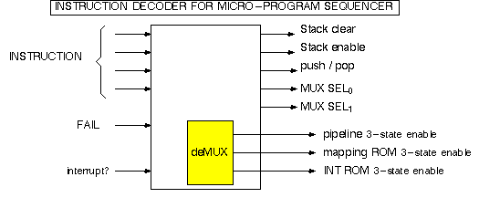
The decoder does not need a clock. It does not need flip flops. So the final act in the design of a micro-program sequencer, which is the final act in the design of the CPU controller, and the penultimate act in the design of the whole computer, is the realization of a truth table. REPEAT: Once we design the instruction decoder, we're finished with the inner workings of the whole computer. The design of the decoder takes us all the way back to the beginning of the book-the turning of truth tables into combinational hardware.
To actually fill in the gates for the instruction decoder design we need to know the
instruction code. In one of the end-of-� exercises you are given an 8-instruction, 3-bit
code and asked to work out a complete design. Here we bring out 6/16 of the 4-bit code +
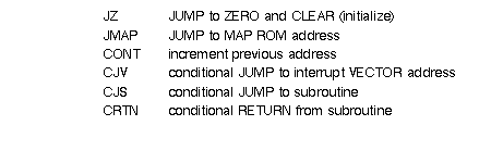
FAIL lines from the 2910 instruction set, for examples.
[We have shadowed the 2910 chip in illustrating the design of a microprogram sequencer, but
we have not shown all of the 2910's features. See data sheets in in AMD book, or JD Lab Manual. In
this regard, one of the problems at the end of the chapter asks about the usefulness of a 4th MUX
input for repeated looping. In the MUX-select options below we've added a 4th choice, ZERO.]
I3 I2 I1 I0 are the instructions bits for the sequencer. If FAIL is active, then the second
condition on JUMP address and stack operation is enforced. The stack has 4 operations:
CLEAR, HOLD, PUSH, POP.
Table of instructions:
|
I3 I2 I1 I0
|
|
PASS
|
|
|
FAIL
|
|
|
|
INST
|
MUX SEL
|
JUMP
Addr
|
STACK
|
JUMP
Addr
|
stack
|
|
0 0 0 0
|
JZ
|
zero
|
|
clear
|
|
|
|
0 0 1 0
|
JMAP
|
JUMP
|
MAP
|
hold
|
|
|
|
1 1 1 0
|
CONT
|
CONT
|
|
hold
|
|
|
|
0 1 1 0
|
CJV
|
JUMP
|
VECT
|
hold
|
CONT
|
hold
|
|
0 0 0 1
|
CJS
|
JUMP
|
PL
|
PUSH
|
CONT
|
hold
|
|
1 0 1 0
|
CRTN
|
POP
|
|
POP
|
CONT
|
hold
|
where the sample instruction abbreviations stand for

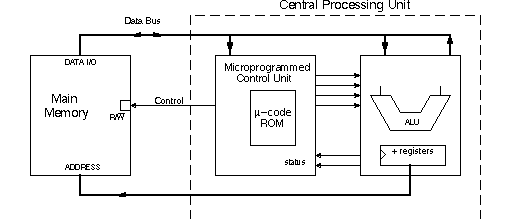
S5 / 4 Connection of CPU to main memory (semiconductor RAM)
The "ultimate" hardware step in our assembly of a complete computer is hooking up
the CPU to main memory. Main memory (called in the past "core memory") will have orders
of magnitude more locations than the cache memory inside the CPU, and will be arranged
as random-access read-and-write cells, as you saw in the Memory Chpt. For the
purpose of the example to be shown here, we assume that the number of bits in the data
path of the CPU is sufficient to address main memory. If the data path is 16 bits, then there
are 216 = 65,536 locations in main memory. Main memory has three parts which need
connection to the CPU:
� Address pins
� Data pins, for both input and output
� Read - write control.
Consider main memory in the form of DRAM chips-slower than the static RAM of the CPU
cache. For connection to main memory a few more registers will be needed; they will be
housed in the CPU.
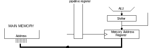
Start with CPU connection to main memory address. Another register-the Memory
Address Register, MAR-which receives its input from the shifter, is dedicated to
addressing main memory. Another bit is added to micro-code to control when MAR
accepts a new address.
Registers near the ALU can store the program counter and data pointer (locations in main
memory of the user instruction currently being executed, and the data being computed
upon), and these values can be passed out to the MAR during a FETCH cycle of the
machine. While the CPU is busy carrying out a user's instruction, the MAR faithfully holds
the correct place in memory.
Next consider the memory data pins, and read-write control. We assume the main
memory data bus is bi-directional, and that whether memory contents are being read
from or written to is determined by the R/W pin on main memory.
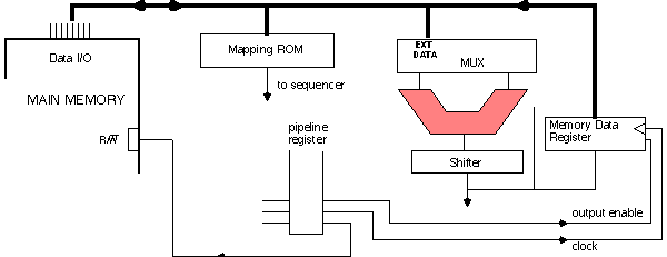
When main memory is in the READ mode, there are two possible destinations-the
mapping ROM or EXTERNAL DATA port on the ALU MUX. As long as the MAR output is
stable, registers are not needed in front of either of these destinations. It is the responsibility
of the microcode to send the output of the mapping ROM into the m-code ROM at the
beginning of each user instruction, but once that is done the CPU control unit doesn't need
to worry about "saving" the contents of the mapping ROM. Likewise, when microcode
decides that data from main memory is needed, it can FETCH the data through a change in
the MAR, then accept the data through control of the ALU MUX select.
Writing to main memory is another matter. Presumably something at the output of the
shifter should be sent to a memory location, so the shifter needs connection through a
3-state device to the main-memory data bus. Three-state enable is controlled from the
pipeline. On the same microcode operation the pipeline register can switch the memory
from READ to WRITE mode. That we have opted to structure the 3-state device as a
register clocked from microcode give the system some latitude in making sure the data
meets thold of the main memory write cycle; the issue is explored more in an end-of-�
exercise.
In hooking up main memory to the CPU we have not dealt with secondary issues such
as addressing modes, main memory being "slower" than the CPU, direct memory access
and how main memory may be loaded from disk drives. But what we've done is sufficient to
make a working computer, given enough intelligence and "width" in the microcode. At this
point we can summarize a computer with a block diagram which includes the three major
components and their interconnects:

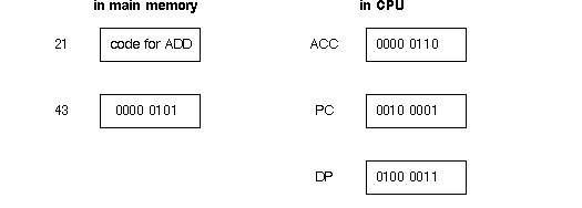
S5 / 5 Example of a user instruction in microcode.
Before summarizing this chapter, we tread lightly into the realm of software.
Let's demonstrate how a particular user instruction could be handled by microcode.
Try the ADD instruction, ACC z ACC + RAM
"Replace the contents of register ACC with the sum of the current ACC and a number
stored in memory location RAM."
Where ACC is stored in a register near the ALU, and the address of RAM is stored in a data
pointer (DP) register near the ALU.
There is another register near the ALU, called Program Counter (PC), which contains the
address of the user instruction ADD ACC to RAM.
For specifics, say that "6" is in register ACC, 21 is in register PC and 43 in register DP, and
that at main memory location 21 is the user code for ADD, and at location 43 is "5".
With apologies to strict register transfer notation, here is what we expect to happen during the ADD instruction. We assume the architecture developed during this � carries out these actions.
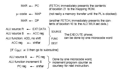
Two FETCHes, two EXECUTES and a test for carry out; 5 cycles of microcode. Should the instruction end with a MAR z PC, or should that be the beginning of the next instruction?
[At the end of the instruction more than incrementing the PC register may need to be done, such as microcode which enables interrupts, inspects their status, services them if they are active, then disables them before starting the next instruction.]
Without setting up all the fields (SOURCE, FUNCTION, DESTINATION, CARRY-IN,
MAR CLOCK, etc) with position codes, we can't fill in the 1's and 0's of the various
microcode words, but this outline is close to the final product-a microcoded user
instruction.

S5 / 6 References
Chapter 4, "Microprogram sequencing devices," of G.J. Myers, Digital System Design with
LSI Bit-Slice Logic. John Wiley & Sons, New York, 1980. Discusses the 2910, plus similar
chips from other manufacturers.
John Mick & Jim Brick, Bit Slice Microprocessor Design, McGraw-Hill, New York, 1980.
Chapter II, on microprogrammed design, goes over features of the 2910.
Wilkes, Maurice, Memoirs of a Computer Pioneer, MIT Press, 1985.
Wilkes originated the idea of microprogramming.
John von Neumann and the Origins of Modern Computing, by William Aspray, MIT Press
(1990). [ review by G. Tweedale, in Nature, Feb. 21, 1991, page 662. Von Neumann had such influence
on the design of early computers that machines like the one we've designed in this � are called "von
Neumann machines." ]
S5 / 7 Summary
- The aptly named computer is a central processing unit (CPU) + main memory.
- The CPU consists of an arithmetic-logic-unit (ALU), shifter, assorted registers and a
control unit.
- We outlined a particular architecture for the ALU section of the CPU, inspired by the 2901
and featuring an input-selecting MUX feeding the ALU inputs. One of the choices of the
MUX was the data output of a small fast "cache memory".
- The ALU + registers require control over ALU source, function & destination.
* A pipeline register in the control unit holds in parallel all the bits needed to control
the ALU & registers; a status register send information about overflow, etc back to the
control unit for use in conditional branch instructions.
- The pipeline register, which may be many bits wide, clocks in a word from microcode
ROM. Sequences of words in m-code ROM carry out machine language instructions;
The entire ROM contains the instruction set of the computer, in somewhat the same way
that DNA contains the protein synthesis code of an animal or plant.
- The next address of the m-code ROM is generated by a sequencer, whose output is a
MUX which selects from four inputs:
CONTINUE, which is the next address after the current one;
JUMP, which in turn can select from the pipeline, a "mapping ROM" with
user-instruction information, or the address of an interrupt service routine.
POP, which returns the ROM to the main program after a subroutine;
ZERO, used in initializing the CPU.
- Subroutines can be nested, thanks to a last-in, first-out stack whose address is derived
from an up-down counting stack pointer.
- The current microcode word in the pipeline register contains the next instruction for the
sequencer MUX, and the choice of what to do next can be influenced by other feedback from
the status register. The instruction decoder in the sequencer realizes a truth table; examples
of instructions from the 2910 sequencer were given.
- The connection of main memory to the CPU requires a memory address register and a
memory data register. The MDR is used for writing to main memory. If main memory is to be
read, its contents go either to a mapping ROM or one of the MUX inputs above the ALU.
- The instruction circuit in sequencer can be realized with combinatorial hardware.
- Several types of instructions were discussed, from the high-level programming language
instructions of the user to the instructions used by the microprogram sequencer when it
decides what the next address of m-code ROM should be. An example of a user instruction,
with FETCH and EXECUTE phases, was given.
S5 / 8 How it ends
We have ended the Supplemental Chapters by giving you insight into a full-featured
sequencer, in the service of a micro-programmed computer. We found that instructions to
a microprogram sequencer were decoded by a combinational logic circuit which realizes a
truth table. At this point we have wrapped around to the beginning: The textbook started
with an exposition about the means to turn a truth table into a logic circuit.