S1 Input-Output Relationships for Logic Gates
----------------
Link to End of chapter Exercises:
S1 / 1 What next?
Up to now you've studied combinational and sequential design, culminating in
general-purpose N-bit counters which can step through any sequence of length � 2N.
You have a solid foundation in logic analysis and design. Now which way to go? The first
impulse is to fly right for the topic of Memory. But in order to understand how to gang
semiconductor memory chips together into memory systems, you must know what a
"3-state output" is. And if we're going to detour for understanding of 3-state output, we
might as well appreciate the scenery of chip outputs in general, including open-collector
output. And once the mountaintops of output have been climbed, the valleys of input can't
be far away. All things considered, we might as well acquaint ourselves with the whole
territory of logic gate input-output relationships, and logic families. Take this chapter, and
next, as a guidebook. Here in this Supplemental Chapter you will
D learn the parameters for static performance listed in manufacturers' IC data sheets;
D study how noise margins are calculated from a gate's voltage parameters;
D appreciate how current flow into and out of chips determines fanout;
D classify outputs as totem pole, open-collector, or 3-state.
In the next chapter dynamic performance of logic chips will be considered, especially
propagation delay of signals from input to output. Comparison of the two major categories
of logic families--TTL and MOS--will be made.
Some development in this and the next chapter presumes you remember the difference
between voltage and current, and what Ohm's Law is. If you don't then review. See the first
part of �1 for help.
S1 / 1 / 1 Hardware can be tinkertoys
You should appreciate that logic design as such is virtually independent of the
hardware used to implement it. Logic, including flip flops, can be realized by optical,
pneumatic, biochemical or even tinkertoy*
parts. We're assuming in this text that, because
of its low cost, high speed, small size and widespread use in modern technology, digital
electronics in integrated circuits is the form of choice for creating logic in hardware. It is
rather vague and abstract continually to discuss and design logic systems with no
reference to hardware implementation. The present � removes some vagueness from
subsequent development and introduces you to the basics of practical digital electronics.
In the text chapter 1 you were introduced to switches as a logic hardware primitive. You
saw that a switch is characterized with a control input threshold. When the threshold is
crossed the switch changes from open to closed, or vice versa. We will use a switch in a
gate as a model from which to discuss voltage levels between gates.
Before we begin to show how well a gate's output can fit as the input to another gate we
must clarify the relationship between logic values of LO and HI, and voltage levels available
to a chip for representing LO and HI. [Terminology note: In this chapter we will commonly refer to
"chips" instead of "gates" to emphasize the importance we are now placing on actual voltages and
currents from real integrated circuit versions of logic gates.]
A riddle: What is a

see end of chapter for answer...
S1 / 2 Logic values from voltage levels
Standard logic families*
operate with a +5 volt to 0 volt (ground) range of potential.
Non-overlapping voltage ranges must be selected for logical 0 and logical 1. It would
seem a straightforward task to declare
LOGIC 0 = {0 < V < 2.5 volts} and
LOGIC 1 = {2.5 < V < 5 volts}.
A linear inverter could then be imagined to have the following output as a function of input:
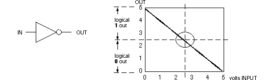
This hypothetical inverter has no margin for error around 2.5 volts input, and no way to insure that voltage levels are kept away from 2.5 volts. By "error" we mean an output of 1 when 0 should have occurred, or vice versa. We can order a solution to this problem by defining a "not-allowed" zone on our 0-5 scale:

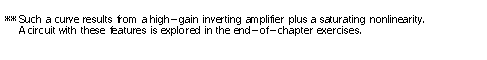
What will keep the inverter output away from the not-allowed zone most of the time is a non-linear IN-OUT characteristic**
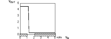
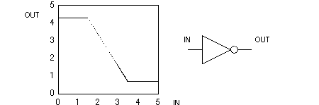
, looking perhaps like this function,
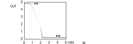
where a steep negative slope moves OUT rapidly (as a function of IN) from one level to another. Using the above graph we can see that when an output is in the acceptable LO range, its value is always about 0.2 volts, and when an output is in the defined HI range, its value is always about 4.8 volts. If the output of a chip with this characteristic is the input to another chip with this characteristic, then separation of logic levels in assured. The only issue not addressed by this curve is how fast the switching from one state to another occurs.
S1#1--can logic levels overlap? what about small 0 & 1 zones?
S1#2--2 B or not 2 B
S1#3--gain and saturation question
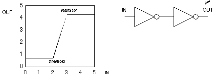
S1 / 2 / 1 Voltage-sensitive switch and inverter
Example 1. In chapter 1 we were introduced to single-pole switches as basic
hardware elements. The simplest single-pole switch was the single-throw version. Let's
place a SPST switch in an inverter gate where input and output voltages can be defined and
studied.
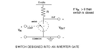
The 3 pins of the switch are labeled "CONT," "common" and "out." Common is shared by
both input and output voltages. Voltage from CONT to common determines whether the
switch is closed or open (voltage-sensitive switch). By the specification (given in the
figure) for switch closing we see that the circuit acts as an inverter. When input is low then
output is high voltage. If control threshold q = 1.2 v, then the input/output characteristic
becomes:
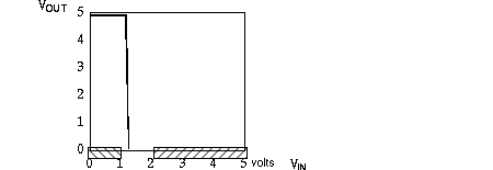
Notice how sharply the I/O curve changes from high to low output as a function of VIN. If we
define logical 0 to be less than 1 volt, and logical 1 to be greater than 2 v., then we have
completed the specification of this inverter gate. We can add more realism to the circuit by
including an offset voltage inside and a "load resistor" outside:
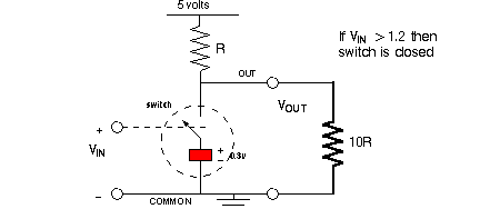
Now when the switch is closed VOUT will be 0.3v instead of 0 v, and when the switch is open
10/11 of 5 volts will appear across the VOUT terminals (out to common). The I/O curve
becomes:

S1#4--I/O curve for 3v inverter
S1 / 2 / 2 One inverter driving another
The load resistor which caused the HI level output to droop in the previous example
mimics a second gate attached to the output of the first. There are two questions to ask
about one gate driving another: (1) Will the receiving gate absorb or deliver too much
current for the first gate to maintain proper logic levels? (2) Even if the second gate has a
low current requirement, will the voltage changes from the first gate be able to flip the
switch of the second gate? We defer the first question until a later part of �8 on fanout; we
finesse the issue by declaring that the gate under consideration has a high input
resistance. One way to think about high input resistance: Even when the control voltage is
HI, little control current is required to keep the switch closed.
S1#5--calculation with input and load resistance
When the load resistor is replaced by another inverter circuit, as shown below,
VIN2 = VOUT1.
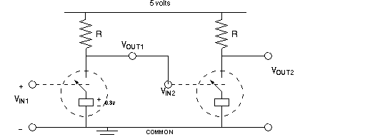
Allowing that the second inverter input requires little current to keep the switch closed, then from VIN1 to VOUT2 we have created a "non-inverter." But depending on the I/O curve of the basic inverter there may not be such an un-eventful result.
Consider the following inverter curve. The curve's shape is right for an inverter, since
it's monotonically decreasing over the 0-5v input range.
No matter what we define to be the voltage ranges for LO and HI, since the lowest output for
this inverter is 2.8v, the output of the second inverter will always be 3v. For example, if we
define LO to be less than 3 volts and HI to be greater than 4 volts then only the first inverter's
output could be LO or HI. Even that requires connecting the first input to ground to drive its
output HI. But when the first inverter tries to drives another with the same I/O relationship
the output of the second gate will always be 2.8 volts. And since the output of the first gate is
the input of the second, the second gate output is always the same-2.8 v. This curve
cannot be an I/O curve of a useful inverter. The output is too high during the LO phase.
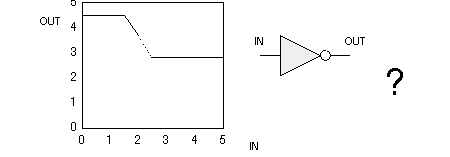
We can create an "inverter" curve with the opposite problem:
In this case the output is too low. It never rises above the lower threshold of 2v for the curve.
If one gate drives another the second output will always be 2.2 v., even if the input of the first
gate is grounded. These "pathological" curves are not completely fabricated-we'll see
them arise later in calculation of fanout, when we load a normal gate output with too many
other gate inputs.
S1#6--will an inverter curve work for an odd number in series?
S1#7--will 2 inverter curves work for inverters in series?

Let's return to a healthy normal and (in this case) symmetric I/O curve for an inverter.
We've given this curve a less sharp break between HI and LO. When two gates, each with
this curve, are in series, the second output can give a correct "non-inverter" output.
If IN = 0, OUT = 0.5; If IN = 5, OUT = 4.4. Shown below is the complete I/O curve for two in
series:
Notice that the slope of two in a row is steeper than the single inverter curve; the threshold
and saturation points are closer together. For the single curve the slope at IN = 2.5 has a
value -2; in the two-in-series curve the slope at IN = 2.5 is -2 x -2 = 4.
In both cases, OUT = 2.5 for IN = 2.5. The second inverter has "cleaned up" the shallow
slope of the first. Again, nothing is said here about how fast the switching takes place.
S1#8--what are inverter outputs for 2 INV in series?
S1#9--which inverter curve is better?
S1#10--design an inverter, given a switch
S1 / 2 / 3 Inverters and feedback
We can learn more about compatible logic levels by studying inverters connected in a
ring. Recall feedback circuits from the flip flop chapter 5. What happens to logic levels in the
following circuit? Notice that the output of one is the input of the other inverter.
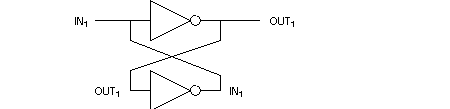
We can draw two inverter curves on one graph to see how the connections match up, and
see where the system is stable and unstable.
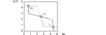
One curve has the expected IN-OUT shape while the other is an "inverted inverter" curve
in which the input is on the vertical axis. The second curve represents the first output as
input to the second inverter, to account for the feedback loop. Imagine the original curve
drawn on a transparent sheet, turned over, rotated 90� then superimposed on the
undisturbed curve. You'd see what's shown above. Only where the two curves intersect are
there possible solutions to the connected values of IN and OUT. Circled intersections H and
L are the stable solutions for binary logic levels. The third solution "U" where
IN = OUT = 2.5 volts is unstable. It's unstable because any small deviation from
(OUT1, IN1 = 2.5, 2.5) will tend to push the circuit towards one of two stable states "H" or "L."
Point U is the metastable state of the flip flop, a state which we discussed at the end of �5.
S1#11--try superimposing curves for the curves of problem 6
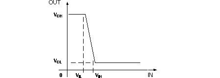
S1 / 3 Voltage parameters for input and output
For an inverter, label (by cross-hatching) the OUT and IN voltage axes with
reasonable specifications of logic levels:
Zero is shown as the minimum; usually 5 volts is the maximum. Any voltage within the HI
range of input can be considered VIH, and any within the LO input range VIL. In data books
for chip specifications VIL is listed as a maximum, and VIH as a minimum. For example, a
7400 chip has VIL-max = 0.8v and VIH-min = 2.0 v. To function properly, our inverter
requires that an input within the LO range guarantee an output in the HI range, and vice
versa. For example, If IN is greater than VIL-max, then output cannot be guaranteed to be in
the HI range (for an inverter). A proper inverter curve must therefore make a transition from
box A to box B. Each box is is as wide as the LO range and as long as the HI range. An
example of a proper inverter curve is shown below:
Keep in mind that the output of one chip is likely to become the input to another chip. For a
good input we would like something considerably less than VIL-max or considerably
greater than VIH-min. On the graph above we indicate a separate concern for output
levels. In order to maintain the guarantee of HI output for LO input, etc, we can shrink the
allowable range of outputs:
The I/O curve above shows output ranges shrunk. Now output voltages have legitimately
separate notation from input ranges: VOH is any voltage in the HI range of output, and
similarly for VOL. A data sheet will list the maximum value for VOL and the minimum value
for VOH.
S1#12--draw a curve with VIL-max = VOH-min
A 7400 chip has VOH-min = 2.4v > VIH-min = 2.0v and VOL-max = 0.4v < VIL-max = 0.8v.
How the limitations of output range are achieved is a matter for a logic chip designer to
work out with semiconductor fabrication. The IC design issue is discussed in [JD Lab
Manual � on electricity, "From electron to chip"]. To switch output from one binary state to another a
gate must spend some small amount time in the forbidden zone between LO and HI. It can be a major
concern of a digital design engineer to insure that no important computations are made when an output is in
the forbidden zone. In combinational circuits the outputs settle to their logical values within nanoseconds
after inputs are presented. In sequential circuits a clock pulse can help insure that outputs and inputs have
synchronized and settled before the next operation is attempted. Then there is the case of metastability,
discussed earlier, in which a flip flop may hang up for a while in the forbidden zone and cause switching
problems.
SUMMARY of voltage parameters (for an INVERTER operation)
VIL Nominally any input voltage such that output is in the HI range. Normally specified as a
maximum value below which output is guaranteed to be HI.
VIH HI level input value above which output is guaranteed to be LO; normally given as a
minimum value.
VOL Output guaranteed to be in logical LO range; VOL � VIL; normally given as a maximum
value.
VOH Output guaranteed to be in logical HI range; VOH � VIH ; normally givenas a minimum
value.
The graph below shows typical relationships between the defined logic levels for 0 and
1, the input voltage parameters, and the output parameters.
Notice that the defined ranges for logical LO and HI must include as subsets the actual
input and output ranges of any particular chip. If all we know about a chip is the I/O curve of
a particular inverter then we can assign the voltage parameters as shown in the plot below.
The various min and max subscripts are implied.
[In S2, on digital-to-analog conversion, we will see a problem created by the fact that logical 0
does not have to be equal to zero volts, and in fact can be as high as VOL. If logical LO not equal to
zero is the input to a digital-to-analog converter, then the converter's output will make a error
proportional to the non-zero value of logical LO.]
S1#13--figure out voltage parameters from an inverter curve
S1 / 4 Calculation of noise margins
All would be well on the highway of digital logic were it not for some major potholes in
the road. Our design vehicle will need shock absorbers. The input voltages we've seen on
the x-axis of our I/O plots can be corrupted by noise, especially in the form of transient
spikes. The noise spikes can be caused by clock pulses sending unwanted current
through the power supply wires, or even by electromagnetic radiation inductively coupling
to conductive loops in the circuit. For now we needn't worry about where the noise comes
from, or even what measures can be taken to shield our circuit or filter noise. At this point we
simply concern ourselves with inverter design virtues which can minimize the effect of input
noise transients.
Look again at a generic inverter curve, reproduced below:
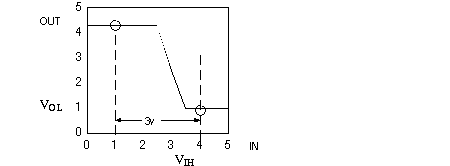
Imagine the input to the inverter is 1v, as circled as VOL. (1v is the output of the inverter at
the logical LO level.) A 1v input results in a HI output of 4.3 v. Now suppose a "noise spike"
of 3v adds to the 1v input. Due to IN = 1+3 = 4v the output drops down (perhaps
transiently) to 1v-a mistake. What defines the minimum size of the noise spike which will
cause such a LO to HI an error? If the spike moves input from VOL to VIH, then the logic
level of the output will change. Therefore DVL, the low-level noise margin, is
if it's functioning properly
DVL = VIH - VOL
a positive number. The "low level" in low-level noise margin refers to low-level input. VOL
is subtracted because the actual low level input voltage in any case is VOL, not VIL.
Suppose the inverter output from the curve above had been held LO by an input of 4.3v.
If a noise spike of -2.3v were subtracted from the input then a HI-to-LO error would
occur on the inverter output. The minimum size noise spike for such an error is DVH, the
high-level noise margin, which, by the same reasoning used above, can be calculated
from
DVH = VOH - VIL
Again, a positive number. And again VOH is used as the actual input voltage, because we're
presuming that a similar inverter is driving the one in question.
If the inverter curve were sharper, then VIL � VIH. For what value of VIL � VIH would
the two noise margins be equal? At �(VOH+VOL). And here's a simplified way to think
about noise margin: The width of the not-allowed zone in the definition of logic levels from
chip voltages. The formulas for noise margins given above calculate transitions from one
logic level to another; formulas for calculating transition from logic level to "undefined
region" are given in an end-of-� exercise, for comparison.
S1#14--another definition for noise margins
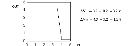
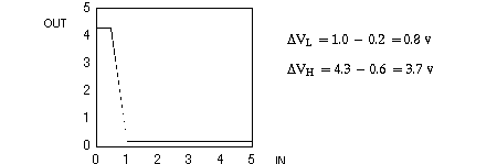
Example 2. How can we improve noise margins? Inspect the formulas above and see
that increasing the difference between pairs of input and output voltage levels will increase
noise margins. Here's an inverter curve which improves DVL, at the expense of DVH:
Here's a curve which does the opposite, improving DVH, at the expense of DVL:
S1#15--calculate noise margins of 4 inverter curves
S1 / 4 / 1 Noise margins of inverters with hysteresis
We can achieve optimal immunity from noise spikes by combining the two I/O curves
shown above, in a hysteresis relationship:
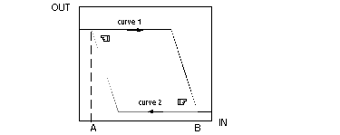
When input starts out less than A, then as input increases, curve 1 is followed, preserving a
good low-level noise margin. When output is HI, the only dangerous noise spikes will be
large positive-going ones. Once input exceeds B, then curve 2 is followed as input
decreases. Curve 2 preserves high-level noise margin when danger from
negative-going noise exists. Hysteresis can be seen in the 7414 inverter chip, where the
hysteresis effects are called "Schmitt triggers."*

Calculations of noise margins for hysteresis: There is no ambiguity with VOL or VOH in
the formulas for DVH and DVL . For VIH use the input level marked with -> on curve 1 in the
diagram above; for VIL use the input level marked with <- on curve 2 in the diagram above.
For example, if VOL = 0.2v and VOH 4.1v and
"B" = VIH = 4.5v and "A" = VIL = 1.0v, then
DVL = VIH - VOL = 4.5 - 0.2 = 4.3 volts and
DVH = VOH - VIL = 4.1 - 1.0 = 3.1 volts.
The sum of the noise margins is greater than 5v, thanks to hysteresis!
S1#16--analogy: noise margin is to voltage parameters as
S1#17--calculate noise margins for 7414 data given
S1 / 4 / 2 High-level voltages when TTL chips drive CMOS chips
If we look in data sheets at the voltage parameters of the two most widely used
standard logic families, TTL (transistor-transistor logic)*
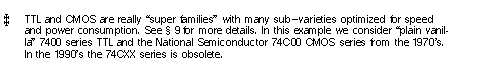
and CMOS (complementary
metal-oxide-semiconductor), we find the following values:

See the high-level voltages in bold. Consider a TTL inverter driving a CMOS inverter.
A CMOS chip needs a minimum high-level input of 3.5 volts, yet TTL is guaranteed to
deliver only 2.4v. (A kind of negative noise margin!) Now it often turns out that a TTL chip off
the shelf does have a high level output greater than 3.5v. But in general a "level shifting"
amplifier may be needed for TTL-to-CMOS interface:

We'll see later in this chapter that an open-collector buffer can be an excellent
level-shifter for high-level outputs.
S1#18--Calculation of noise margins for mixed logic
S1 / 5 Inputs-Maximum, minimum and floating
In the preceding discussion users of ICs were cautioned to make sure input levels
avoided an undefined zone between the regions for logical LO and logical HI. There are two
other regions to be avoided--inputs below 0 volts and above VCC (usually 5v). Such
out-of-range inputs could come only from sensors or other circuits outside of the logic
system, but their effects must be guarded against. For TTL chips, inputs less than -0.5v or
greater than about 7 volts (depending on the TTL family) can cause permanent damage to
a chip. Look under the data sheet category of "absolute maximum ratings" of the chip in
question to find exact values. These out-of-range input voltages must be applied for a
minimum amount of time to be damaging. Thousands of volts of static electricity can spark
a TTL input and do no harm because the gate input can dissipate the charge. Not so with a
CMOS input, which can be zapped by static electricity. Modern CMOS inputs are protected
to an extent by reverse biased diodes, but caution must still be exercised when handling
CMOS chips. More later, and in Lab Manual.
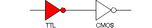
Floating inputs. What if an inverter input is connected to nothing? You might think the
input would be scored as a logical 0. Surprisingly, in some logic families-particularly
TTL-an unconnected input will usually seem like a HI input. You can't count on the floating
input to stay high, though. Noise spikes from clock pulses are capable of shifting
unconnected inputs momentarily from high to low. The spikes are coupled to inputs by
minute capacitances in a circuit's wiring. The circuit below, featuring our voltage-sensitive
switch, suggests a way in which an unconnected input may float high:
If VIN is grounded, or connected to a low-level output, then logical LO will be forced on the
input; otherwise the input will appear HI (unless spooky noise spikes pull it down
transiently.) The temptation to not connect inputs usually comes with multi-input NANDs,
NORs, etc, or with asynchronous SET and RESET on flip flops, but once a logic gate
becomes involved in a logic circuit all its inputs should be accounted for and those not
connected to some external input or other chip output should be tied to VCC or ground.
CMOS chip inputs float unpredictably if they're unconnected. Sometimes an
unconnected CMOS input will maintain an initial value for many seconds then drift slowly
from one logic state to the other as temperature changes slightly. It is always good practice
to tie unused CMOS inputs to VDD or ground. VDD (where "D" stands for drain in an MOS
transistor) can be as low as 3 volts in some CMOS families. CMOS chips from the 1970's
(4000 series, 74CXX series, could tolerate up to 15 volts on supply voltage.
S1#19--tie a TTL input to +8 volts?
S1 / 6 Current parameters for high and low voltage levels
To continue our dissection of a chip (an inverter in particular) we must consider the
current*

associated with input and output voltage. Fortunately, we have only four basic
voltage conditions with which to associate currents:
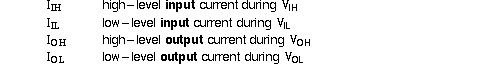
Convention has it that a positive current flows into the gate in question, as shown below.
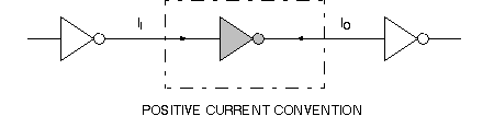
Consider the input currents, IIH & IIL.
The data sheet for a TTL 7400 chip says IIH = 40 mA = 40 x 10-6 amps.
40 mA is the maximum amount of current which will flow into a 7400 NAND gate when one of
its inputs is held HIGH.
The 7400 data sheet also says IIL = -1.6 mA = -1.6 x 10⁻³ amps. Why the negative
sign? Because when a chip's input is held low, current will flow out to the driver on the left.
Notice also that IIH is 40 times smaller than IIL. [You'll understand the reason for |IIH| < |IIL|
when you study the structure of a TTL gate's inputs and outputs, shown at the end of �8.] Knowing
VIH and IIH we can attempt to calculate an input resistance RIN:
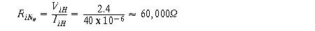
This calculation is not entirely correct; for one thing the input of a logic gate is a
semiconductor junction, which cannot be modelled by a simple resistor; for another the
actual VIN may be more like 4.8v than 2.4; for another we really want to know the slope of the
function I(V), dI/dV = 1/ZIN, (where Z stands for impedance) at V = VIH. All that said, we can
remark that the answer is in the right ballpark and that the input of a
switch-as-a-TTL-inverter does not allow much current in. The input impedance is
great.
Output currents IOH and IOL. We want to specify output current parameters by
showing how the gate can deliver or absorb current without exceeding the limits of the
logical state the output is in. To understand this point of view, start with our
voltage-sensitive switch, now with resistors in both the path to +5v and the path to
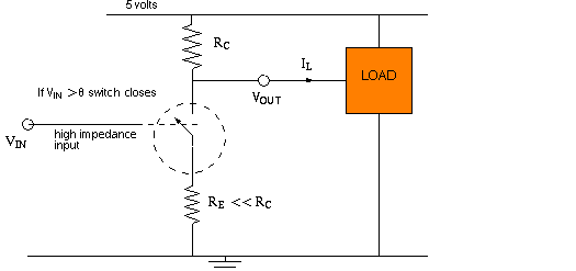
ground, and a "load" with access to both +5v and ground:
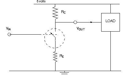
Admittedly this model is not too close to actual working of an IC inverter; nevertheless, in
the case above, the switch is open (Vin LO) and the inverter is trying to stay HI. Current flows
out through RC. If the switch were closed, VOUT should be near ground and therefore
RE << RC in this model. Generally output current capability is an order of magnitude
greater than the corresponding input current requirements. We'll see this difference
exploited in the next part, where fanout is calculated.
S1#20--current parameters as a function of temperature
S1 / 7 Fanout calculated from current parameters
A data sheet for the 7400 chip says that IOH is -400 mA. The minus sign reminds us of
the convention for labeling current flow out of a chip. If the chip had to deliver more than 400
mA, then too much current I would flow through an internal RC and the voltage drop RC�I
would be too great to maintain VOUT = 5 - RC�IOH > VOH. In the output HI state all the
current flowing out to the load must pass through RC, so the Ohm's Law voltage drop
RC�IOH represents, in our first-order model, the burden of the load on the output voltage.
Normally we expect the load to be other logic gates all connected to the output in question:
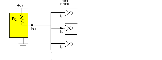
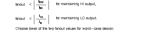
But we know that a chip input in the high state takes in IIH = 40 mA of current. Therefore if more than 10 gates are tied to one output, and you wish to maintain that output in a HI state, you're out of luck. The circuit won't work; the maximum "fanout" is 10. The 11th gate would require bringing IOUT to 440 mA and the total current to flow out of the chip in question would exceed the IOH maximum, therefore:

where fanout is the number of gates one output can project to before failure. So far we've considered only failure from HI level output strain.
Fanout from IL values. The data book for the 7400 chip says
IOL = +16 mA = 0.016 amps, meaning that a 7400 input held low sends 16 mA to the gate
which is driving it. Again, if some resistor to ground RE sees the IOL then a voltage RE�IOL
will pull the output away from 0v and the defined range of LO. Since IIL = -1.6 mA, again we
find a "worst case" fanout of 10

The current flow looks like:
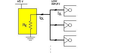
with the output gate being a "sink" for current from the sources of low-level input pins.
Why do high-level inputs send out current? Again, the answer lies at a level of detail we've
not yet considered; the figure earlier, illustrating a bias resistor and a floating input,
suggests a origin for low-level current leaving an input.
Official fanout is the worse of HI level and LO level fanout calculation. *
S1#21--fanout of 7414
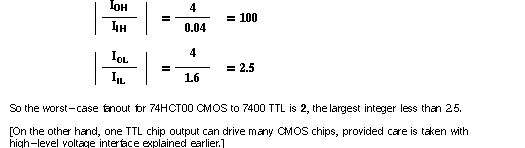
S1 / 7 / 1 Fanout of CMOS to TTL
In the previous sub-section we saw problems with noise margins when TTL projected
to CMOS. Now we will see limitations of fanout when CMOS drives TTL. To start with, the
formulas we developed for fanout of one chip to other chips in its logic family work equally
well for fanout calculations between logic families, as long as you're careful to read
properly the current parameters from the different families. In the case of a CMOS chip
projecting to several TTL gates, the data sheet for a CMOS chip (the 74HCT00 quad NAND
gate from Texas Instruments
) * says that
IOH = -4 mA & IOL = 4 mA
What are the corresponding II's for 7400 series TTL?
IIH = 0.04 mA & IIL = -1.6 mA
Calculating HI and LO level noise margins you find
S1#22--CMOS fanout calculation
S1#23--TTL and CMOS interface fanout problem
Dynamics of fanout. It is worth mentioning, without going into detail, that a major
limitation in fanout can be the output current required to meet the guaranteed tpd ,
propagation delay of a chip. In a TTL chip, each input can have as much as 3 pF (10-12 F) of
capacitance and can require something like � mA of drive current to switch a gate in about
10 nsec.
If a longer propagation delay of the gate can be tolerated, lower output drive current can be used.
S1#24--Delay caused by fanout buffers
S1#25--is a 4-input NAND one load or 4?

S1 / 8 Output and loads on logic chips
So far in this chapter outputs, like inputs, have been described by their current and
voltage parameters for HI and LO logic states. Outputs, however, do have fundamental
differences from inputs. For one, many different inputs can be connected together, in
anticipation of acting on the same signal at the same time (the start of parallel processing).
Connecting outputs together, though, would not seem to make sense. What if one output is
HI and another is LO when two are connected together? Will sparks fly?
Another example: Outputs must be capable of delivering or absorbing considerable
current, in order to drive loads, particularly the inputs of other logic gates. Outputs
therefore have an order of magnitude lower "Thevenin equivalent impedance" than inputs.
Lower output resistance can be seen by comparing II's and IO's, (much greater IOL and
IOH) or by going through the calculation of output impedance we did earlier for input
impedance.
show a realistic load here:
Output of an inverting switch. Here's the last model we used for an inverter, attached
to a load. We show resistances RC and RE to help describe the effects of output current.
If input is LO (switch open) then current can flow only through RC to the LOAD. VOUT must stay higher than VOH in order for the output voltage to qualify as a logical HI value. Using Ohm's Law across RC we find VOUT = 5 - RC�IL, where IL is the load current. The worst case for VOUT as a HI would be a short circuit from output to ground:

Where IL = 5/RC and VOUT = 0, a ruinous condition for logical HI!. The range of possibilities for VOUT and IL is shown below on the "load line," where a resistance RL is inside the LOAD box. The case of RL = 0 is circled.
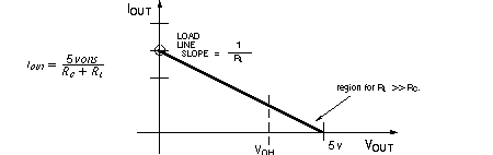
The calculation for IOUT is shown below.
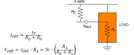
In practice we hope RL >> RC (to maintain the difference between input and output mentioned above). If RL is large compared to RC then VOUT � 5 volts, as required by logical HI. How could RL shrink, and thereby endanger a HI-level status of VOUT? If many LOAD's are connected in parallel to VOUT (the problem of fanout):
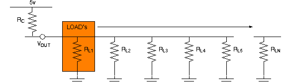
Imagine each RL associated with a different gate's input. N equal resistors RL in parallel have an effective resistance of RL/N. As N increases, RL/N will eventually decrease enough to force VOUT below VOH.
S1#26--load fanout calculation for pullup resistor
S1 / 9 Open collector output
As you can see by inspecting the box presented later in this �, an actual TTL gate has a
transistor-resistor combination where we show the collector resistor RC in our simplified
diagram above. It's possible for several gates to share one pull-up resistor RC if RC's are
deleted from the gates and replaced by a load connected to +5v. Gates which can share
one external pull-up are said to be open collector. An open collector gate looks rather
foolish by itself:

Isolated collectors can sing only one note-a LO note. Connecting a resistor from the collector to +5v gives the open-collector output a chance to sing HI. Standard outputs are not to be connected to each other but the next example shows the benefit of tying together open collector outputs in the cause of wired-logic.
S1 / 9 / 1 NOR gate with OC inverters
Example 3. An N-input NOR gate can be realized with N open-collector inverters.
The next figure (a) shows two inverter-gates sharing the same pull-up resistor. The
designer must make sure the external pull-up resistor RPU is much larger than the internal
resistance in the path to ground, modeled by RE. If so, when either of the switches is ON
(closed) then VOUT drops below VOL. The following truth table results:
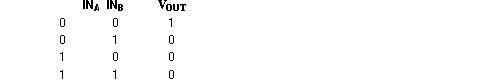
which is the truth table for a 2-input NOR. An N-input NOR could be realized with N
open-collector inverters tied to a common pull-up.
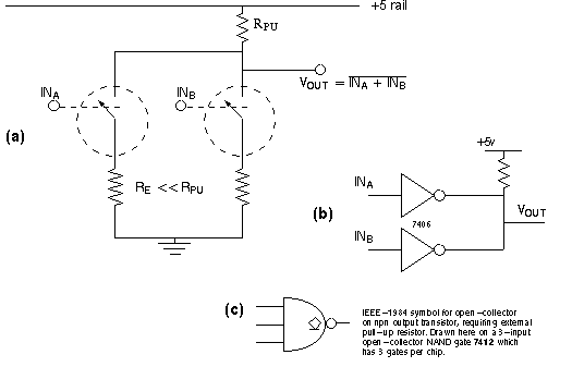
In (b) of the figure we show 2 inverters of a 7406 hex open-collector inverter chip tied
together; In (c) is a 3-input NAND gate with open-collector output, shown with the
IEEE-1984 diamond symbol for open-collector output requiring pull-up resistor.
Example 4. What logic function is achieved by the following open collector gate
circuit? Remind yourself of what path current follows to ground through RPU when the
switch in the gate is on.
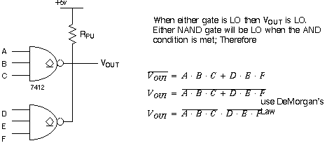
S1#27--What is the logic function determined by OC NORs tied together?
S1#28--Wired-AND. re-draw NOR as AND circuit
S1#29--A six OC inverter circuit to analyze
Standard TTL gates have a built-in pull-up pathway with a properly designed
resistance. When you use an open-collector chip you must make sure the current flowing
through the pull-up resistor is less than the maximum the gate can handle, and that the
voltage drop across the pull-up resistor is less than what would drop VOH below the
threshold for logical HI. An end-of-� exercise takes you through the calculation for RPU
for a 7406 gate.
S1#30--Problem calculating min and max for 7406 R-PU
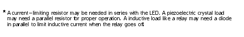
Even one open collector output by itself can be useful in interfacing a logic system to an
external load. If the load is an LED or a relay or a piezoelectric crystal the designer doesn't
have to worry about logic levels of high and low outputs, but must make sure the load does
not allow more than the maximum allowable current to pass through the open collector
transistor.
Example 5. Each of the six inverters in a TTL 7406 chip has an output transistor
specially designed to handle 30 volts and sink 40 mA, much more than the absolute
maximum ratings of a standard TTL output. Thanks to its specs you can tie a 7406
output-through a load-to some larger positive voltage, say + 15v. Shown below is a
7406 controlling an LED. Notice that the 7406 itself is powered by +5 volts, but its output is
able to be pulled up to +15v. The LED comes on when IN is HI.*
The output of the 7406 in
this case is not intended to drive other TTL logic gates; its high-level output would be
greater than the absolute maximum input rating of a gate input!

S1 / 9 / 2 A multiplexer with open collector NANDs
Example 6. By tying together the outputs of NAND gates which are enabled by
SELECT inputs, the final OR gate of a multiplexer can be eliminated. See below for a 2!1
MUX version.
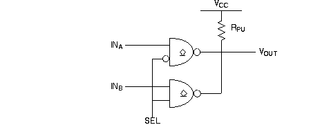
Only one NAND at a time will be selected. The NAND gates not selected will be pulled up HI
on the common output line. If the data input to the selected NAND is HI then the selected
NAND's output will pull VOUT LO. A common wire connected to several gate outputs is
called a bus. The bus wire is highlighted above.
S1#31--4 to 1 MUX using OC NANDs
S1 / 9 / 3 Current parameters for OC chips
What meaning does IOL have for an open collector output? In the data sheets of 7406
IOL is described as having only a "max" value, which is the maximum amount of current
allowed through the output transistor. For the 7406 IOL = 40 mA, much greater than the 16
mA for a standard TTL chip. What about IOH for an open collector chip? IOH is the leakage
current which can flow through the output transistor when its off and the output voltage is
held high by some external means:
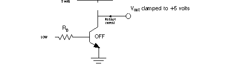
For the 7400 chip IOH is listed at -400 mA, whereas for the open-collector 7406 IOH is
+250 mA. Why the difference in sign? If the gate output has a built-in pull-up resistor, then
current moves through the pull-up resistor to the load, otherwise current leaks from the
HIGH load back into the open-collector transistor. Leakage current is an important
consideration when calculating the maximum value of RPU; leakage current must flow
through RPU when the transistor is off and the output is trying to maintain a HI value; if RPU is
too large then too much voltage drop = RPU�Ileak will knock VOUT below the minimum value
for logical HI.
S1#32--why can a 7406 drive a 7414 with no pull up?
S1 / 10 Totem-pole output
An inverter output can be balanced between VCC and ground by placing switches
between both:
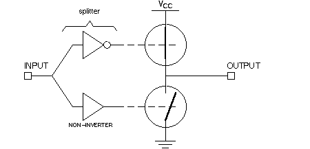
The input must pass through a "splitter" which makes sure the two switches are not closed
at the same time. (What would go wrong if both switches were closed at once?) In the inverter case
above, INPUT is LO and OUTPUT is HI. In actual practice, the switches are transistors, and
associated with each transistor-switch will be a current-limiting resistance.
What advantages does a totem pole output provide over a
single-switch-with-resistor output? Basically the advantage is one of switching speed.
By replacing a linear resistor with a non-linear transistor, a low resistance (faster) pathway
appears when the output needs to switch from LO to HI. When the output needs to revert to
LO status, the transistor turns off and becomes a high resistance path. At the same time a
low resistance path to ground appears, thanks to the bottom transistor switch.

S1 / 10 / 1 Box: Transistors in a TTL NAND gate
Assuming you know something about bipolar junction transistors, this box presents the
inner workings of a standard TTL gate.
The circuit below shows a complete TTL NAND gate (7400) with totem pole output. All
transistors are npn. the input transistor T1 is has 2 emitters, functioning as inputs. In the case
shown the inputs are allowed to float HI, so the chip output is LO. When the inputs are not
connected to ground then current from the 4K resistor above T1 can flow to the base of T2,
turning T2 on. When the splitter transistor T2 is on, the bases of the two totem pole transistors
T3 and T4 are within 0.2 v (VCEsat) of the same voltage. The diode between the two totem pole
transistors places another 0.7 v between the totem pole emitters. Enough current passes
through the 1KW RE to keep T4 on, at a VBE of 0.7 v. In that case T3 stays off because its emitter
voltage is too high (0.7 + 0.2 v) with respect to its base voltage, which is also 0.9 v.
[Question: What would go wrong with the TTL gate if the totem pole diode were replaced by a
short circuit?]
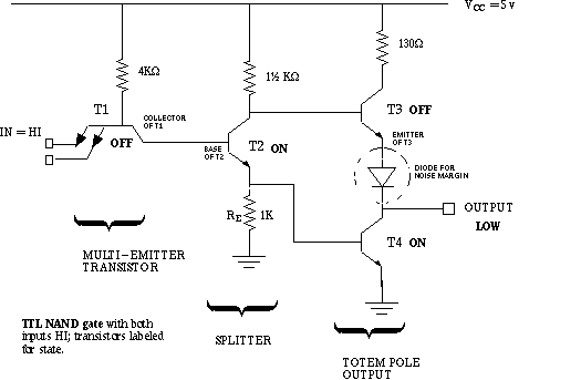
If T2 is off, from lack of base current, then the base voltage of T3 is high enough to keep T3 on. T4 stays off in this case because no current flows through RE to generate a turn-on voltage for base-emitter of T4.
The 130W resistance above T3 is the minimum size required to limit output current in case
the output pin is grounded when T3 is on, or during those transients of switching when both T3
and T4 are on simultaneously. In fact the � 30 mA of current which passes for a nanosecond
from VCC to ground during TTL switching is a source of noise on the power lines, and should
normally be damped by external bypass capacitors placed from VCC to ground at various
locations in a TTL logic system.
[Question: What will be the logic level of the output if both T3 and T4 are on at the same time?]
Sedra, A. & K. Smith, Microelectronic Circuits, 3rd Edition, HRW/Saunders, Phila. 1990.
See chapter 13, part 3, pages 1003-1022.
S1#33--what happens if the TTL gate stops at T2?
S1#34--transistor operating curve and load line
S1#35--Darlington pair question

S1 / 11 Three-state output
We saw that a totem pole output should avoid the condition when both its switches are
closed at the same time, or excess current will flow from the VCC rail to ground. But what if
both switches are open at the same time? Then the output isn't connected to anything in the
chip. It looks like a "high impedance" (Hi-Z) to any attached load. This state of
dis-connection is the "third state" (the other two being 0 and 1) for a 3-state output. The
diagram below shows a way for an "enable" control to determine if an output goes into the
Hi-Z state.
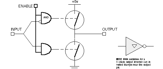
The circuit in the diagram above will be a standard inverter when ENABLE is HI [the two
AND gates will be enabled]. When ENABLE is LO, as shown, both AND gates are disabled
and both switches are open. The output is Hi-Z.
S1#36--analysis of 3-state disabled gates
At first glance it must seem that the Hi-Z state is even less useful than an open
collector output-at least the open collector output had a chance to become 0. However,
like the open-collector output, the virtue of 3-state output shines when outputs are
connected together.
When tying several 3-state outputs together you need to insure that only one output is
enabled at one time. The one wire to which all the 3-state outputs are connected is called a
bus. Look at the following arrangement of four chips. CS is the active-low enable for each
chip output; connecting the four outputs of an active-low de-multiplexer to the CS's
guarantees that only one of the chips controls the bus at any one time.
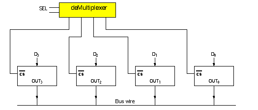
The other three outputs are in a high-impedance state and offer no load or signal for the chosen output to compete with. Notice that as a unit the circuit above acts as a multiplexer. One DATA output at a time is sent onto the common bus wire.
We saw earlier that open collector outputs can be tied together in a multiplexer-like
bus. Compared to open-collector busses, 3-state busses offer some advantages. (1)
The 3-state devices can be separate from the enable-controlling circuit, whereas the
open-collector design requires N-input O.C. NAND gates to serve in the role of
multiplexer. (2) The leakage current of a 3-state device is less than the leakage current of
an open collector gate (20mA vs 40mA, for example) (3) The user of a 3-state bus is not
limited to a protocol in which active signals must be LO, as he or she is with an open
collector bus.
Example 7. One-wire I/O with 3-state buffers: Suppose, instead of using a pin for
input and a pin for output on a chip, the same pin is used for both input and output,
depending on the mode of operation (read, write). One can use 3-state buffers to connect
two internal lines to one external line:
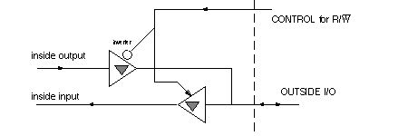
Say the 3-state buffers have active-low enables; then if control is HIGH the "inside
output" signal is enabled onto the I/O pin and the "inside input" pin is disconnected (Read
mode). If control is LO then the I/O data has access to the "inside input" and data can be
transferred to an internal register.
S1#37--bidirectional transceiver with 3-state devices
S1#38--making a 4-to-1 inverting MUX out of a 74LS240 3-state buffer
S1 / 11 / 1 Static parameters for 3-state outputs
Is the Hi-Z state output really disconnected from the chip? No, but not much current
can flow into or out of the chip when it's in the Hi-Z state. Just how disconnected a chip can
be is described by a parameter IOZ, the off-state output current. IOZ is the amount of
current which can flow into a chip's output when the chip has had its output disabled. In
data sheets IOZ is often given as IOHZ and IOLZ, where IOHZ is the current flowing into an
output with a specified HIGH output voltage applied, and IOLZ is the current flowing out of
an output with a specified LOW output voltage applied. In the case of the 74LS240 3-state
inverting buffer
IOHZ = 20mA and
IOLZ = -20mA.
S1#39--question about fanout from a disabled 3-state gate
S1 / 12 Summary
- To convert voltage levels into binary logic values: Divide a voltage range, say 0-5 volts, into
a logic-LO region, a logic-high region, and a "forbidden" gap between the two regions.
- Input voltages of a chip must be able to swing the output into the LO or HI regions defined by
the user. Input specifications in a data sheet are VIL, the maximum low-level voltage, and
VIH, the minimum high-level voltage.
- Output levels. On an inverter inputs less than VIL must guarantee the output will be in the
logic-HI range. A chip data sheet will say the HI output won't dip less than VOH. Likewise,
a low-level output will never be more than VOL if inverter input is greater than VIH.
- Noise margins are how much change in input voltage can occur before a chip changes output
level.
Low level noise margin is DVL = VIH - VOL.
High-level noise margin is DVH = VOH - VIL.
These are conservative margins for transition from one logic level to another, not from a
logic level to the forbidden zone.
Hysteresis in the I/O curve can provide for both large DVH & DVL margins.
- Input currents: To hold an input voltage below VIL requires supplying an input current IIL to
that terminal. If IIL < 0, as it is for TTL, then current has to flow out of the input to ground. To
hold an input above VIH requires suppling an input current of IIH.
- Output currents: A gate with its output at logic HI can supply a current up to IOH without its
output voltage falling below VOH. A gate with its output LO can conduct a current up to IOL
from its output to ground without its output voltage going above VOL.
- Fan out. Divide appropriate output current by input current to calculate how many gates one
output can safely drive.
- Input and output voltage and current vary from one logic family to another; special care may
be needed for CMOS chips to fan out to many TTL chips. Chip outputs should not normally
be tied together, except for-
- Open-collector outputs, which must be pulled up by an external load, and can allow the user
to (1) interface from one voltage level to another (2) design "wired-AND" functions (3)
Create OC multiplexers whose common outputs can form a bus.
- 3-state outputs feature a third high-impedance state in which the output is electronically
disconnected from the rest of the chip. If care is taken to insure only one at a time is not in the
Hi-Z state, many 3-state outputs can be tied together on the same bus wire.
Answer to riddle: Volts-wagon pulling a mobile Ohm.
References for further reading (good for �9 too):
David Winkel & Franklin Prosser, The Art of Digital Design, Prentice-Hall, Englewood
Cliffs, NJ, 1980. Chapter 12, "Meeting the real world."
and Herbert Taub & Donald Schilling, Digital Integrated Electronics, McGraw-Hill, New
York, NY, 1977. Chapters 1 and 4-8 contain a wealth of information (somewhat dated in 1991) about
semiconductor devices and logic families.
Wakerly, John, Digital Design Principles and Practices, Prentice-Hall, 1990. See chapter 2.
Ward, S.A. & R.H. Halstead, Computation Structures, MIT Press/McGraw-Hill, 1990,
chapter 1, "The Digital Abstraction."
S1 / 12 / 1 Logic vs hardware
In the same way that knowing command line attributes for a compiler can help you
assemble an applications program, knowing chip specifications can help you design and
troubleshoot a digital circuit.
The material in this � and the following one is significantly different from that of the first 7
�'s. For the preliminary part of some digital designs, you don't need to worry about what's
in these two chapters on chip parameters; it's possible to deal with preliminaries of logic
design without having to know the input-output parameters of particular chips. The
manufacturers of integrated circuits go to great trouble to make the chips "user
friendly"-a direct connection from an output pin to an input pin is all that's needed in most
cases. However, to understand open-collector and 3-state outputs, and to squeeze the
most out of any design, especially when optimizing speed, power consumption & noise
immunity, it's essential to have a grasp of chip I/O attributes, including logic levels. At the
least, this � and the next should help you read data sheets for chips more intelligently.
The concept of 3-state output is needed in order to understand memory chip output
"busses" for large memory systems.
What you are learning in chip I/O chapter is applicable to standard logic family IC chips
(which have been emphasized here) and to gate arrays and other large-scale
repetitive-structure hardware which the user can program on a custom basis.
S1 / 13 Box: TTL gate input and diode logic
Shown below is the transistor arrangement for a TTL NAND gate input. Notice that, for an
output projecting to one of the inputs, the load of a TTL input looks like a resistor in series with
a diode (the base-emitter junction). The multi-emitter structure may seem a little surprising
as an input if you are used to seeing the base as the input. In this case the multi-emitter
structure helps make TTL gates switch faster; there is little concern about current gain.
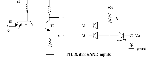
The multi-emitter structure should remind you of the �1 diode AND gate, recalled on the right, with an additional diode from T2 base-emitter junction. For the multi-emitter, if the inputs are grounded then T1 turns ON and T2 turns OFF. T2 is a "splitter" which projects to a totem pole output structure. T1 is a multi-emitter structure, fabricated with IC technology. If both IN's are high, then base current flows through the collector-base diode of T1 into the base of T2 and T2 goes on. What if IN's aren't connected to anything? (if they "float"?) The current T1 goes into the base of T2. The gate acts as if the inputs are high-unconnected TTL inputs float high. Attaching a volt meter to a floating TTL input won't show a value in the logic HI range, instead the value will be near the voltage of the base of T2-a value in the indeterminate range. Only a change of 0.1-0.2v is needed to make the output LOW. In fact noise spikes can turn on T1 transiently, if its inputs are unconnected.
NOTES:
Show where 3-state control intercepts TTL
J&K, p.92-schematic of 3-state TTL gate.and see Wakerly (I), page 106.
need GRAPHIC on CMOS input. CMOS inputs don't necessarily float high;
their input impedance is so large they'll remain in whatever state
they pop into; they're even more susceptible to noise spikes than
un-connected TTL inputs. Maybe put it in the lab manual...
Often a real chip will have better fan-out than calculations from the data sheet current parameters
suggest. However, practical designs must work under all conditions (temperature, etc) with any chip
in a lot. It is not acceptable practice to try exploiting the limits of functionality shown in the best chips.*